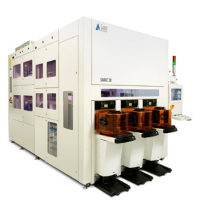
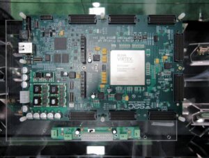
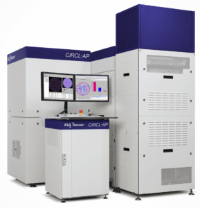
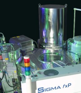
As Si interposer and 3D stacked memory devices enter into production, albeit in low volumes, semiconductor manufacturers are lining up their ducks to be ready for high volume manufacturing (HVM) when it happens. As a result, some suppliers of high volume manufacturing equipment who have been rather quiet through the development phase are now showing their cards. For example, KLA-Tencor recently introduced its line of advanced wafer level packaging (AWLP) inspection and metrology tools to the market, targeting both 3D IC and fan-out wafer level packaging (FOWLP). CIRCL-AP is a fully automated platform that integrates wafer front-side and edge inspection and review. The ICOS T830 component inspection system completes the wafer-to-package process control offering. I recently sat down with Lena Nicolaides, VP and General Manager, SWIFT Division, KLA-Tencor, to get her take on the FOWLP and 3D IC markets, and also learn more about KLA-Tencor’s activities in this space.
The Back Story
When asked to define KLA-Tencor, Nicolaides doesn’t use the term “equipment manufacturer,” rather, she says: “We are a process control company that provides inspection and metrology solutions to our customers. We help customers improve yield, which helps control cost.” The company, which was formed in April 1997 through the merger of KLA Instruments, an inspection company, and Tencor Instruments, a metrology company, is well known for its expertise in front-end process control. Combining inspection with measurement provides an overall loop for improved process control, explained Nicolaides.
In 2008, KLA-Tencor acquired ICOS. The recent introduction of the CIRCL-AP and ICOS T830 completes the evolution to offer wafer and component inspection in the back end.
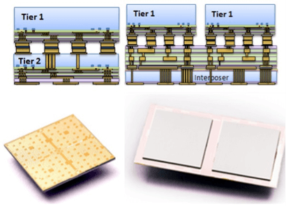
Although it may appear that KLA-Tencor is new to AWLP, that isn’t the case. The company actually began engagements four years ago with a memory customer who saw solutions in the company’s CIRCL (which stands for concurrent inspection and review cluster) wafer inspection platform for 3D IC processes. “They asked us, ‘can you modify the CIRCL system to provide inspection at certain process steps for 3D IC?’” recalled Nicolaides. It turned out that because the middle-end-of-line (MEOL) processes specific to 3D ICs aren’t typical back-end processes, their front-end tool could measure critical steps that other systems were blind to. The company placed 3 systems customized for 3D IC with the customer, and has also since engaged with various consortiums including imec and IME, all geared towards TSVs and higher end applications.
Ironically, although FOWLP is taking off faster than 3D IC in manufacturing, KLA-Tencor’s platform was first developed for 3D IC processes, noted Nicolaides. Then as FOWLP ramped to production and manufacturers were looking for ways to lower cost and improve yields, they realized that technologies developed for 3D IC could be implemented for FOWLP. “We found ourselves able to provide solutions to the OSATs,” noted Nicolaides.
The IoT Impact
“We are benefiting from the Internet of Things (IoT)” said Nicolaides. Initially, she sees demand for FOWLP growing on the consumer product side, but as device functionality becomes more complicated, 3D will be required. For example, the automotive market is a huge growth area for semiconductors overall. According to IC Insights, there is already $425 worth of chip content per car, and this number is expected to double over the next 5 years. Moreover, car manufacturers are already looking at 3D. At ISS Europe in February, a representative of Audi announced that TSVs will be in automotive electronics “very shortly.”
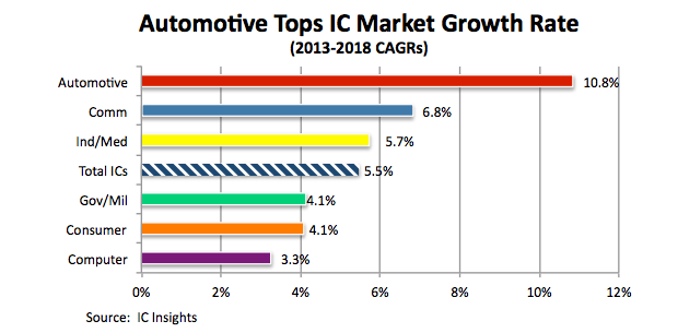
Of the six major end-use applications for ICs, the automotive IC market is forecast to experience the strongest average annual revenue growth rate through 2018. (source: IC Insights)
“The automotive industry is all about zero defects,” explained Nicolaides. “We have to inspect every die and every wafer.” As such, automotive manufacturers are willing to pay more.
How Do We Lower Cost?
In the OSATs world cost is king. Improving yield and automating inspection processes are two ways to lower manufacturing cost, regardless of the device being built. Historically, inspection requires operator review of many images to find defects. Nicolaides explained that what the OSATs are looking for is a way to improve yield at a reduced cost by reducing the number of images needed, as well as the number of people required to review them.
“You can’t improve yields if the systems you’re using are blind to killer defects,” said Nicolaides. “Customers are coming to us saying they need better sensitivity and better capture rate. This is music to our ears because we already have solutions to enable the industry, even for 3D IC, to make it cost effective.”
Nicolaides further explained the advantages of automated defect inspection and binning that are the hallmarks of the CIRCL-AP and ICOS T830 systems. Sensitivity and capture rates help with yield overall, and when it’s automated, the results are more consistent and require fewer operators to perform the inspection. “Customers looking for automated tools are an indication that we’re headed to volume production,”
A comparison study between manual inspection and automated inspection proved that the automated tool not only found more defects of interest (DOI) than manual operators, it could also classify and bin them by defect type. In the study, one operator found 10 defects. A second operator found 30. The tool found 50. Additionally, there were few common defects between the two operators, but the tool found them all.
Not all are killer defects, said Nicolaides, some just require improved processes to eliminate them. Systems without a good capture rate can generate a lot of “noise;” capturing something that’s not real. 50% of these are not real, and require many operators to review them and decide which are real. Nicolaides explained that with the CIRCL-AP, the capture rate is high, eliminating the need for manual review. High throughput means fewer tools. All this translates to lower operating expenses.
“When we were entering the market, many players didn’t realize the differentiation between the defects,” noted Nicolaides. “The timing for us is phenomenal. We’re coming in at a time where the industry is looking to reduce cost, while additionally looking to next-generation requirements.”
Defining Volume Production for 3D IC
“Customers looking for automated tools are an indication that we’re headed to volume production,” noted Nicolaides. A memory company is setting up a pilot line for memory stacking. It may be small volumes, but it’s still HVM for them. “It’s enough to consider it HVM,” commented Nicolaides. “And it’s more than people would have expected. 3D is transitioning and we fully believe in the next few years we’ll see more because the functionality and performance that comes from 3D IC is incomparable.”
Nicolaides predicts that four years from now, we’ll see 3D ICs in more devices as costs continue to be improved. “The inflection point that’s happening today involves improving overall cost and yield in the backend,” noted Nicolaides. “KLA-Tencor can play a role in that—that’s what excites me.”
Even if it would be relegated to high performance computing and memory, the growth of 3D IC in these two areas of the industry is sufficient to make it worth the investment. ~ F.v.T.
The post Executive Viewpoint: The Impact of Process Control on FOWLP and 3D IC appeared first on 3D InCites.


 Nordson ASYMTEK’s programmable Tilt + Rotate 5-Axis Fluid Dispenser dispenses using 5 axes instead of 3. The X and Y tilt enables dispensing from a vertical position, varying tilt angles to all sides of a component and up to the top of a 3D stacked die with high precision and positional accuracy.