Quantcast
Channel: 3D InCites
Viewing all 2184 articles
Browse latest View live

IFTLE 454: TSMC Exhibits Packaging Prowess at Virtual ECTC 2020

$
0
0

I cannot say I enjoyed this year’s COVID 19 version of ECTC 2020, but I guess it was better than nothing. I will leave the discussion of what I would like to see improved in the software package for the organizers.

Let’s first take a look at three key papers presented by TSMC whose goal, it is obvious, is to become the King of Advanced Packaging.

InFO-SoW Packaging for High-Performance Computing

In this paper, TSMC attempts wafer-scale integration with its integrated fan-out (InFO) system-on-wafer (SoW) packaging technology. In many ways, InFO-SoW is reminiscent of the early 1980s attempts by Trilogy to create a full SoW. This modern solution attempts to eliminate the substrate and the printed circuit board (PCB) by serving as the carrier itself. They note that their main driver for such a system is high-performance computing (HPC) as we enter the exascale computing area. The perceived advantages of InFO-SoW are shown below (Figure 1).

InFO SoW packaging

Figure 1: Key advantages of InFO SoW package. (Courtesy of TSMC)

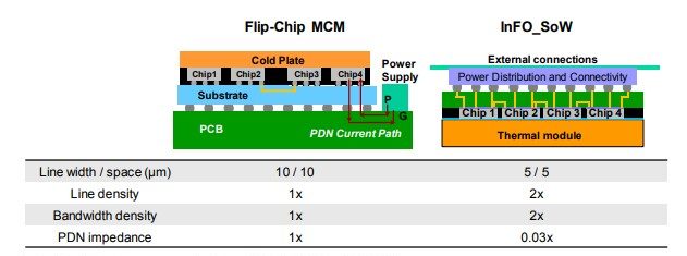
In Figure 2, TSMC compares InFO-SoW to what they call a “regular flip-chip multichip module (MCM).”

FIgure 2: Flip chip packaging compared with InFO SoW. (Courtesy of TSMC)

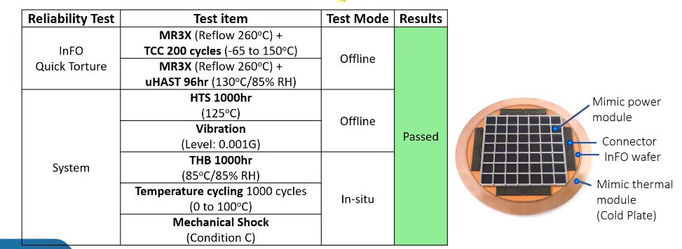
For flip-chip MCM, the signal has to pass through PCB and then back. Not so for InFO -SoW. In addition, to get an RDL length of 20mm, the InFO solution shows a 0.4 dB lower loss at 28 GHz resulting in a 10% power savings. The lower loss is due to the lower roughness of the substrate. BUT …In comparison to traditional motherboard configuration, the INFO SoW must distribute more heat per unit volume and therefore must use a liquid cooling solution. InFO-SoW reliability testing is shown in Figure 3.

Figure 3: Results of reliability testing (Courtesy of TSMC)

Chip-package interconnect (CPI) risk assessment was done using finite element analysis (FEA) to compare the stress in the extreme low-K (ELK) dielectric layers compared to successfully qualified-flip chip architecture equivalents. ELK stress of InFO-SoW is 60% lower than that of the flip-chip structure due, they presume, to the thick compliant dielectric layers of the InFO.

In conclusion:

Ultra High-Density SoIC (SoIC-UHD) with sub-micron Bond Pitch

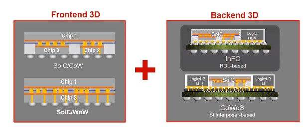
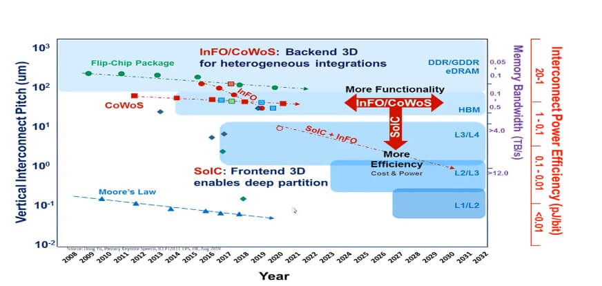
SoIC was first introduced by TSMC at last year’s ECTC Conference. With the goal of continuing Moore’s Law, TSMC explains its advanced packaging used for both back-end and front-end 3D. Back-end 3D refers to existing fan out and interposer packaging technologies. Front-end 3D refers to chip-to-chip stacking whether it is chip-on-wafer or wafer-on-wafer. The reason they call SoIC front-end 3D is that it is based on wafer processing. This makes it possible for their chip-to-chip interconnect density to go down to < 1µm pitch (Figure 5)

front-end 3D vs 3D packaging

Figure 5: Illustrating the difference between front-end and back-end 3D. (Courtesy of TSMC)

Things that affect the bonding yield include cleanliness, optimized Cu topography (from CMP), and Cu barrier optimization. Optimizing each resulted in ~ 30% yield improvements.

Bonding pair resistance and breakdown voltage are extremely sensitive to overlay. Only when the overlay is less than 0.1µm will resistance be minimal and stable.

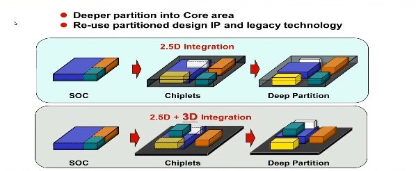
So, what could this bonding be used for? They contend that this will enable chiplet partitioning and subsequent reintegration. Ultra-fine pitch bonding allows a deeper partition and reintegration (Figure 5).

chiplet packaging

Figure 7: Deep partition into the core area by re-using design IP and legacy technology nodes. Re-integration can be 2.5D or 2.5D + 3D depending on the system requirement and the best cost-benefit. (Courtesy: TSMC)

SoIC can also be used for multilayer stacking. Specifically, TSMC detailed its technology called Immersion-in-memory compute (ImMC) which “interlays logic and memory by stacking.” One would optimize logic and memory separately, get known good die (KGD), and then stack as shown in Figure 8.

packaging vs. front end

Figure: Front-end 3D, SoIC, multi-chips, multilayers stacking enables new compute architecture. Flexible 2D and 3D layout with close chips proximity. Immersion ImMC is an example. (Courtesy of TSMC)

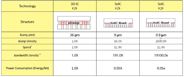
The chart below compares the traditional 3D IC using solder bumps vs SoIC using 9µm and 0.9µm pitch densities.

The density and power efficiency of the TSMC branded technologies are shown below.

SoIC for Low Temp, Multilayer 3D Memory Integration

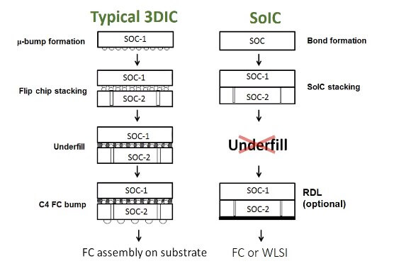
This paper focused on multi-layer memory stacking, comparing the integration flow between typical 3DIC package and SoIC package. Since SoIC is a bumpless structure, it can achieve a much tighter pitch and it does not require any underfill processing (Figure .

Bump density, electrical, and power/thermals are compared below:

LT-SoIC 3D memory reportedly outperforms typical 3D memory stacks due to the smaller form factor, higher bandwidth, and lower power consumption.

It becomes obvious that this TSMC technology will be in competition with Xperi DBI technology for memory stacking in the coming years. IFTLE will be keeping an eye on this competition.

TSMC Builds $10B Packaging Facility in Hsinchu

Focus Taiwan has reported that TSMC will open a new high-end integrated circuit packaging and testing plant ($10.11 B). The plant will be built in the Chunan section of Hsinchu Science Park. It is scheduled to be completed in May 2021, and operations will start in mid-2021. TSMC already operates advanced IC packaging and testing plants in Taoyuan, Hsinchu, Taichung, and Tainan.

For all the latest in Advanced Packaging stay linked to IFTLE……………………….

The post IFTLE 454: TSMC Exhibits Packaging Prowess at Virtual ECTC 2020 appeared first on 3D InCites.


FCC-approved BLE and LoRa module includes Antenna in Package

$
0
0

In engineering school, I learned that different laws of physics apply when the widely used electricity with 50/60 Hertz gets into the Gigahertz or even Terahertz range. In the decades since, I have managed to keep a safe distance to this challenging world of radio frequencies (RF) needed for transmitting data wirelessly. With Antenna in Package (AiP) becoming an important topic for advanced packaging, my luck ran finally out. I now find myself studying again RF physics: Insertion loss, modulators, mixers, S-parameter models, impedance matching, attenuators, types and characteristics of filters, etc. – so I can better understand the challenges as well as benefits of AiP for higher levels of integration.

The Evolution Toward Antenna in Package

At the June 17 MEPTEC & iMAPS webinar, Chris Barratt, the co-founder and CTO at Insight SiP, located in Southern France, described their evolution towards AiP (Figure 1). He demonstrated his many years of RF experience, outlined the strengths of the Insight SiP team – pictured above – and explained how easy their FCC approved modules make it to transmit data wirelessly. As a backbone of his presentation and example for their products, Barratt used one of their RF modules, the ISP4520. It’s designed for Bluetooth Low Energy (BLE) and Long Range (LoRa) signaling. The integrated antenna supports 2.4 GHz for BLE, 915 MHz for LoRa and is small enough to fit into the 9.8 x 7.2 x 1.7 mm package.

Antenna in Package

Figure 1: Evolution towards Antenna in Package (AiP) at Insight SiP (Source: Chris Barratt, CTO Insight SiP)

Benefits of Using RF modules with Integrated Antennas

As Figure 1 shows, modules with integrated antennas reduce a system’s form factor significantly. The shorter interconnections and lower drive I/Os in a module reduces power consumption and extend battery life. Modules with integrated antennas, like the one discussed here, also enable system design experts to quickly incorporate wireless signaling into their systems – reducing system design time and risk. Depending on the country and regulatory agency (e.g. FCC in the U.S.), every radio has to pass a more or less stringent certification process, before the entire system can be operated in their region. RF modules are either fully or mostly pre-certified and eliminate or minimize such time-consuming and costly certification efforts. Last, but not least, modules reduce the number of components on a system’s bill of materials (BOM), simplifying supply, and inventory challenges.

ISP 4520 Block diagram

Antenna in Package

Figure 2: Block diagram of the ISP 4520 module. (Source: Chris Barratt, CTO Insight SiP)

Figure 2 shows a block diagram with the functions inside baseband SoC and RF transceiver. In addition to the two packaged and fully tested ICs, this figure also shows that a significant number of other parts are needed to complete the module. In response to a question from the audience, Barratt emphasized that he prefers to use fully packaged ICs in a module, because exhaustive testing of bare dice, especially if they contain RF functions, is not (yet) sophisticated enough.

RF Module Design and Verification Flow

Barrett first described the schematic to the layout design process, then extraction and the verification steps. His team uses Altium Designer, Cadence’ Allegro SiP, or Expedition, from Mentor, a Siemens Business, for the design steps. For 3D parasitic extraction, they use Ansys’ HFSS, CST Studio, or ADS’ FEM. They create n-port S-parameter models and feed them, together with the annotated schematics and the models of baseband SoC and RF transceiver, into the Keysight ADS simulator. Then Barrett’s team simulates accurately the interactions between the two ICs, the passive components, the antenna as well as the impact of substrate characteristics on the RF signals. Insight SiP typically uses BT as substrate material. Barrett emphasized: Since using Electronic Design Automation (EDA) tools extensively, they can optimize and verify designs much faster, easier, and more accurately than with traditional prototyping. Also, EDA tools enable them to consider component tolerances, materials characteristics as well as manufacturing variations, to improve manufacturing yields, and performance of their products.

Antenna Integration Challenges

The wavelength of a 915 MHz LoRa signal is 32 cm and a quarter of the wavelength (minimum length the antenna should have) is 8 cm. A 2.4Ghz Bluetooth signal has a wavelength of 12 cm and a ¼ wave is 3cm. Considering that the entire module is less than 1 cm long, it takes RF expertise to “extend electrically” the length of an integrated, in this case, dual-purpose antenna, to meet signal transmission and reception criteria. Figure 3 gives a hint of how extending the length of an antenna works, to fit it into a small package. It also shows the keep-out zone required near an antenna.

Figure 3: Layout of an Antenna in Package (AiP) (Source: Chris Barratt, CTO Insight SiP)

Personal comments

Barrett’s presentation gave a perfect example of the benefits of higher levels of integration. While combining packaged ICs in a module is widely used today, Insight SiP’s extensive use of EDA tools surprised me. Their reasons for not using bare dice confirm what I heard from other designers: Wafer-probe needs to improve further! In addition, SoC dice designers need to include more probe pads, loop-back circuitry, built-in self-test (BIST), and even redundant circuitry, to make it easier for manufacturers to achieve high yielding multi-die ICs.

The value of the Internet of Things (IoT) depends significantly on the amount of data the low-power IoT edge nodes can capture and transmit to the cloud, using BLE, WiFi, LoRa, 5G or other standards. As the use of 5G is taking off in mobile phones, RF experts tell me that multiple RF modules, with AiP, will be needed per phone. Phase 1 of 5G deployment, using sub 6 GHz signaling, is ongoing and doesn’t require many changes to the RF modules. However, phase 2 uses Millimeter-wave signaling, will demand big changes, e.g. accurate data about existing materials characteristics at 60+ GHz and new materials that minimize insertion loss at such frequencies.

What MEPTEC & iMAPS Offer Now and Next

If you want to learn more about Barrett’s presentation, you can download his slides and/or listen to the entire presentation, as well as many previous webcasts, here.

On July 1, Stephen M. Rothrock from ATREG will address the U.S. – China trade war. Register here.

On July 15, Jan Vardaman will give her annual IC Packaging update

For Sept 16 the Known-good-die (KGD) workshop is planned. See more about it here. ~Herb

The post FCC-approved BLE and LoRa module includes Antenna in Package appeared first on 3D InCites.

VLSI 2020: 3D Continues to Dominate Advanced Semiconductor Technology

$
0
0

As a process geek, The Symposia on VLSI Technology and Circuits has long been one of my favorite conferences. The fact that it rotates between Kyoto and Honolulu adds a bit to its attractiveness. However, VLSI 2020, as with most, was held virtually.

Having attended a reasonable share of conferences and presentations this year, I think the IEEE and the VLSI committee did a great job of making this conference available to the attendees, as well as managing the number of speakers and keeping the conference running seamlessly, or at least it seemed that way to me. As a virtual conference, VLSI added a few features that I thought helped attendees get the most out of it and possibly attend some sessions that they may not have if they have attended in person.

One aspect that I particularly like was the executive sessions that the VLSI committee included. These sessions gave a quick two-minute overview, with essentially a live Q&A session, either by the moderators of the session or via online chat. This allowed attendees to get a quick view of the session, get their questions answered, and then decide if they wanted to hear the entire paper.

Moore’s Law Continues in 3D

The advanced CMOS Si session discussed the transistors of the future. Currently, FinFETs are considered to be the transistor of choice through the 5nm technology node. Past 5nm it appears the transistor of choice will move to stacked nanosheets. TSMC and CEA-Leti presented on nanosheet gate all around (GAA). It was a bit surprising that there were only two papers on this topic, and that none of the other logic manufacturers or research groups contributed to it. CEA-Leti presented on a 7-layer GAA structure (Figure 1). Sometimes the lack of industry papers means that they are getting close to high volume manufacturing and they don’t want to tip their hand as to what they are doing.

VLSI 2020

Figure 1. 7 Layer Nanosheet structure by CEA-Leti (Source CEA Leti)

The 7-layer GAA will lead to sub 5nm technology nodes with transistors that have improved gate control and higher DC performance over FinFETs, according to the author Sylvain Barraud. The complexity of processing the GAA nanosheets is complex, so it will be a few more years before this technology is in mainstream production.

One of the possible alternatives, or it might be better to say the evolution of nanosheets, are monolithic transistors. In Figure 2, the IMEC paper presented by Sujith Subramanian demonstrates the transition from nanosheet transistors to forksheet to complementary transistors (CFETs), where the NMOS nanosheet FET is stacked on top of the PMOS FinFET. The argument is that the stacked transistors will significantly reduce the area needed for future technology nodes, thus enabling the continuation of “Moore’s Law” increasing the number of transistors per unit area.

VLSI 2020

Figure 2 Technology pathway for Logic Transistors. (Source IEEE 2020 Symposia on VLSI Technology and Circuits.)

The electrical data looks promising, but the authors have yet to build the entire 3D device. There is the PFET data and the NFET data, but no CFET data; so there is the possibility that the thermal processing of the NFET might have some effect on the PFET. A great deal of work is still needed before this will get to high volume manufacturing, but work by CEA-LETI and IMEC in this space are showing a great deal of promise.

One of the process areas that amazes me in the monolithic 3D integration is the advances in low-temperature epitaxy without anneal. Getting decent device characteristics with epi grown at 525°C is mind-boggling to this old batch epi person. Some subsequent monolithic papers that use laser annealing processes for doping and material annealing suggest that monolithic manufacturing will be mainstream relatively soon, as laser annealing enables the process flow to manage the thermal budget, such that there is little if any damage to the base device, as presented in the CEA-Leti paper on building sequential CMOS devices at 525°C or less. The low-temperature process techniques have opened the door to combining GaN transistors with silicon transistors, as shown by Intel, which can be advantageous in the power semiconductor, and communications devices as demonstrated in the Intel paper using a layer transfer technique for the Si layer on top of GaN transistors. Low-temperature processes were then used to manufacture the Si transistor with no impact on the GaN transistors.

In the distant future, once 3D integration gets neuromorphic compute under control, quantum computing or qubits will enter high-performance computing. While quantum computing will replace some of the high-performance compute applications unless quantum computing can be developed at room temperature, the use in everyday applications such as a mobile phone is unlikely, as carrying around a bottle of liquid nitrogen isn’t really feasible.

More than Moore

3D Packaging or monolithic semiconductors are increasing in importance for both high-performance computing (HPC) in AI learning, and sensors for the IoT. The need for more computing power combined with memory is critical for reducing AI learning time and potentially reducing both the time and energy needed in the learning phase of AI.

In the sensor space, being able to successfully combine, either in package or silicon, improves the performance and can reduce the power of the sensor package. It is also possible to add some additional compute power, thus creating an integrated low power nearly stand-alone sensor system. There was considerable information on the above in the short courses. The goal or challenge is to place as much compute power with the optimum memory power in the same package for AI or HPC applications.

While there was a good deal of information on the heterogeneous packaging in the short courses there were only a few papers on the topic in the conference sessions. TSMC presented one paper in the heterogeneous integration on the HPC aspects of packaging using 7nm processors and demonstrating how to effectively deliver power to the processors and chiplet package. CEA-LETI presented on their ExaNode process for building systems for HPC applications.

As memory is key for HPC figuring out how to increase the amount of DRAM available to the logic in heterogenous packaging is key. In the 3D packaging session, the focus was on memory bandwidth as a key issue for high performance and neuromorphic computing applications. CH Tsai of TSMC presented on the company’s system-on-integrated chip (SoIC) bumping process that will eventually allow for 16 DRAM to be combined into the high bandwidth memory (HBM) stack. Nine is the current technology, and the paper presented 12 memory layers. The micro bump process reduced thermal performance by 7% and 8% respectively in the 12 and 16-layer HBM.

Norio Chujo of Hitachi presented on a bumpless build cube (BBC) wafer-on-wafer (WOW) which uses a through silicon via (TSV)-to-TSV contact eliminating the bumps completely. Chujo used a wafer-level stacking technique that created a 9-layer HBM stack. Chujo is proposed that a 32-layer stack is possible using the bumpless technique. The paper claimed that by eliminating the bumps, the capacitance was 1/20 of a conventional bumping process.

As I close, if I use the VLSI conference to help predict the direction that process technology will move in the next several years. It appears that the industry will continue to focus on smaller faster transistors to continue to facilitate a form of “Moore’s Law”. However, packaging will become increasingly important in the area of both sensors and HPC, as the packaging engineers figure out how to put the devices together in the optimum configuration as business continues to move into the digital realm.  ~ D. Freeman

The post VLSI 2020: 3D Continues to Dominate Advanced Semiconductor Technology appeared first on 3D InCites.

SEMICON China 2020 at a Glance

$
0
0

SEMICON China 2020, collocated with FPD China, was successfully held June 27-29, 2020. SEMICON China was the first big semiconductor industry show held in Shanghai this year since most of the exhibitions were canceled due to COVID-19. And it may be the only SEMICON event we’ll see with physical booths this year globally.

SEMICON China 2020

Figure 1: SEMICON China 2020 Registration Hall

The total square meters of SEMICON China exhibitions exceeded 80,000m2, and there were 1000 exhibitors with 4000 booths. SEMICON China 2020 comprised four main big exhibition areas: IC manufacturing, compound semiconductor, industry technology innovation alliance of integrated circuit materials, and SEMI China Talents Plan. Audiences were also able to visit some booths virtually to learn about the latest products and technology exhibited. Some companies canceled booths before the exhibition because of COVID-19, and instead rented hotel meeting rooms to hold customer meetings and do demonstrations.

Meanwhile, the show featured 20 forums and activities covering areas like chip design, manufacturing, packaging & testing, equipment, materials, etc. Forums were also available virtually for the duration of the live event. During the grand opening forum, speakers including Long Ju, President of SEMI China; Ajit Manocha, President, and CEO of SEMI; Qing Wu, Vice Mayor of Shanghai; Bertrand Loy, Chairman of SEMI Board, Director, and CEO of Entegris; Weihua Cheng, CTO of YMTC; Qing Chu, CEO of UNISOC; Georges Andary, Director of Bosch China Automotive Electronics; Suxin Zhang, President of SICA; etc. all expressed that 2020 is a tough year for semiconductor industry due to the COVID-19 and complicated international situation. But there are also great opportunities. Crisis and opportunities always co-exist.

SEMICON China 2020 Grand Opening Forum

Figure 2: SEMICON China 2020 Grand Opening Forum

During the grand opening forum, Wu said the revenue of the Shanghai IC industry increased by 38.7% in January-May, 2020, even though this year is very special and tough for the industry. Zhang said that 2019 was a tough year for the global semiconductor market, but China’s  IC performance was great, with a 750billion yuan industrial scale, 15% year-on-year growth.

Domestic and foreign companies actively joined different topic forums. KLA, Applied Materials, Edwards, and WillSemi (OmniVision), etc. discussed the cultivation of talents for the semiconductor industry. ST Microelectronics, ADI, and IMEC, etc. talked about MEMS and sensors in the automotive application forum, discussing the innovation and market analysis of this field.

CSTIC, held on June 29th, was also an important forum during SEMICON China. The speakers included Dr. Doug Yu, Research Vice President of TSMC; Dr. Ravi Mahajan, Academicians of Intel; Dr. Anthony Yen, Vice President of ASML; and Dr. Sanjay Natarajan, Vice President of Applied Material, etc. SEMI Best Young Engineer Paper Award and SEMI Best Student Paper Award were also awarded during the conference.

Besides those forms mentioned, there were also forums about advanced packaging, smart manufacturing, advanced wafer manufacturing, memory development, etc. Lastly, officials report that booths for SEMICON China 2021 were sold out. Clearly, people are already eager for next year’s event. We hope to see you there.


The post SEMICON China 2020 at a Glance appeared first on 3D InCites.

What to Expect at Virtual SEMICON West 2020

$
0
0

Some of my SemiSisters; Sarah-Lyle Dampoux, Sharon Rehbinder, Bettina Weiss, and Veronique Pequignat.

This feels weird, folks. For the first time in 15 years, I didn’t board a flight bound for SEMICON West on the Monday after July 4th.  That was expected since the dates got pushed out by two weeks this year. But now that the event will be held virtually, I’m feeling it more. After all, what is July without spending a week in San Francisco in the company of my industry peeps?

But all is not lost. SEMI is doing its best to recreate SEMICON West in the virtual space, with the same high-quality content, as well as a virtual exhibition where you can engage with your peers through live chat in real-time. We will be participating with a 3D InCites virtual booth, and I’ll be viewing the keynotes and executive panels from the comfort of my home office.

It all kicks off Monday, July 20th at 10 am PT. An All-In Pass ($299 for members and $399 for non-members) gets you live programming from July 20-23, 2020 as well as continual 24/7 access to all programs and exhibitors for an additional 60 days. The Expo pass is free and allows you to visit the virtual exhibits in the halls and  SMART Pavilions. That alone could keep you busy for days. Here are some of the highlights to keep in mind.

Improving Responses to Worldwide Challenges

I read SEMI’s press release this morning promoting Virtual SEMICON West, and the above phrase jumped out at me. According to this, “the SEMI team has rallied over 150 semiconductor industry visionaries and government leaders to gather for keynotes, fireside chats, and executive panels to discuss opportunities for improving responses to worldwide challenges.”

Now, SEMI may have already been planning on addressing these topics before the pandemic hit. I don’t know for sure. I do know to celebrate SEMI’s 50th Anniversary was top of mind; and lining up speakers and planning an event of this magnitude takes months of careful preparation. Former Vice President, Al Gore has been listed as a Featured Keynote for a while, which is great, because sustainability is always a timely topic; as is anything to do with Big Data, AI, and Cloud Computing. That’s what he will be talking about with Applied Materials’ Gary Dickerson, and IBM’s John Kelly III. But beyond that, much of what you’ll view was pulled together in the past two months after the world hit tilt, and everything changed.

Therefore, instead of an exciting report about the industry upturn that we all expected to be happening in January, this year’s Market Symposium will focus on the impact of COVID 19 and increasing global tensions; and the Bulls and Bears session will discuss the role microelectronics plays in providing much-needed solutions, respectively.

Additionally, I applaud this team for pivoting to address topics that matter now more than ever, such as changing how we work and adapting to the new norm; as well as critical yet sensitive topics like racial and economic injustice.

Diversity and Inclusion

SEMI’s commitment to Diversity and Inclusion continues, with a full live program that is scheduled to take place on Thursday, July 23, from 10:30-12:30, and three on-demand sessions that will be available throughout the event and beyond. I’m particularly proud to see that three of our 3D InCites Community members (and SemiSisters as well) are participating in this important event: Lam Research, TEL, and FormFactor.

Virtual SEMICON West 2020 Technology Talks

Did I mention there’s enough content here to keep you busy for days? From advanced manufacturing and heterogeneous integration to reliability and test, and all the applications space our industry touches, there is truly something for everyone. Check out this sneak preview for all the details so you can plan your experience.

One advantage of a virtual event is the extended time you’ll have to view all the content. Be sure to pace yourself. My plan is to view the ‘live events’ as they occur during the morning hours and visit the exhibits when they are “staffed” — from 9-3 pm daily (except Monday – 10 am-12 pm) and browse the rest as my schedule allows. If you’re attending, be sure to visit our virtual booth where you’ll find video interviews with a number of our 3D InCites Community members. Read more about that here.


The post What to Expect at Virtual SEMICON West 2020 appeared first on 3D InCites.

Zooming Into SEMICON West

$
0
0
SEMICON West preview guide

Check out the SEMICON West Preview guide at www.semiconwest.org.

This year, 3D InCites is zooming into SEMICON West, talking with our community to see how our members are handling this challenging landscape and to share updates on technology, business, and other news.

Join us in the 3D InCites virtual booth to view Zoom interviews with EV Group, Smoltek, Jiaco, Finetech, FormFactor, Trymax Semiconductor, ERS Electronic, StratEdge, Mosaic Micro, SVXR, Plan Optik, Onto Innovation and Xperi.

Many 3D InCites Community Members are also participating as SEMICON West exhibitors. Here’s an important tip: there are no booth numbers to identify companies this year. However, they are grouped in halls by category. For example, all the equipment suppliers are in one hall, and then listed in alphabetical order. Be sure to stop in to visit!


You’ll also find our members participating in these SEMICON West Keynotes and Executive Panels:

[LIVE] Optimizing Your Manufacturing – Sensing, Connecting, and Predicting the Smart Way

Tuesday, July 21 | 10:30 am – 12:00 pm

Full Stack Computational Optimization Through Virtual Fabrication

10:30 am – 11:00 am

Speaker: Joe Ervin, Director, Semiconductor Process & Integration, Coventor, Lam Research

[LIVE] Manufacturing Excellence – Using AI and Analytics to Put Your Data to Work

Tuesday, July 21 | 12:30 pm – 2:00 pm

AI-Powered Metrology and Inspection for Semiconductor Manufacturing

12:30 pm – 1:00 pm

Speaker: Yudong Hao, Senior Director Marketing, Onto Innovation

[LIVE] The New Reality – Digital Internships

Wednesday, July 22 | 10:30 am – 11:00 am

The microelectronics industry has long relied on internships to help build its workforce. Most interns who successfully complete their short stint at a company are offered a full-time job. Even before COVID-19, more companies have been turning to digital internships to engage students from across the country. Management and internship coordinators had to quickly come up with new ways to not only give interns meaningful work but replicate day-to-day personal and social interaction, considered valuable parts of internships. Deemed an ‘essential industry’, microelectronics continued it crucial work, and interns remain important to meeting future workforce needs.

Speaker: Tina Revels, University Relations Manager, KLA

[LIVE] Keynote: Tim Archer, President and Chief Executive Officer, Lam Research

Thursday, July 23 | 8:30 am – 9:00 am

[LIVE] Creating a Culture of Inclusivity

Thursday, July 23 | 10:30 am – 11:00 am

Diversity can take many shapes and forms. This panel discussion will broaden your vision of what it means when we embrace diversity and how everyone can benefit from the rich skillsets these speakers represent. Panelists will address how to be an ally for women in tech, challenge microaggressions, and reduce power differentials in a professional environment. We will speak to thought diversity in tech, unconscious bias, and how companies can affect change to move the needle for a more inclusive culture.

Speaker: Lubab Sheet-Davis, VP, Innovation and Strategy, Office of the CTO, Lam Research

[LIVE] Hiring Heroes – Creating a Path from Military to Civilian Workforce

Thursday, July 23 | 11:00 am – 11:30 am

Many companies are eager to hire veterans because of their discipline and work ethic. However, transitioning from the military to civilian work can be confusing and challenging. Learn why veterans make ideal employees especially during these uncertain times.

Speakers:

Kathy Garner Manager, Talent Acquisition and Global Mobility, TEL

Shawn Harbert, Sr. Mgr, NPI Materials, PECVD | GOps (Pilot Materials), Lam Research

[On Demand] Building a Better Network: Crucial Connections

Research has shown that women are often more hesitant to ask a connection for anything due to concerns about being perceived as opportunistic, or even weak. Women are generally strong collaborators and communicators, but lack of business-related connections leads to fewer opportunities for recognition and promotion. So, how can women, including women of color build the critical connections which will lead them to succeed? This presentation will explore the vital role networking plays in the success of all women throughout various stages of their careers, as they pursue opportunities and overcome challenges.

Speaker: Amy Leong, Chief Marketing Officer, FormFactor

There are also three Advanced Packaging sessions on-demand, all about heterogeneous integration in different applications. Bill Chen, of ASE Group Global, also a 3D InCites Community Member, will lead those discussions.

For more details about Virtual SEMICON West, visit the website.


The post Zooming Into SEMICON West appeared first on 3D InCites.

SEMICON China – An Exhibitor Perspective

$
0
0

After the cancellation of SEMICON Korea in January, not many were surprised to learn that SEMICON China would not take place in March as planned. After a couple of months in limbo, SEMI finally announced that the big exhibition would be moved to the end of June, during a weekend, and overlapping with the Chinese Dragon Boat Festival – a three-day national holiday. This, however, did not deter people from attending the show, as the venue’s CEO Michael Kruppe could later report: “The show went well, with 30,000 visitors in three days.”

As a company with a dedicated sales office and team in Shanghai, we found ourselves in the fortunate position of being able to attend the show without sending anyone on a plane halfway across the world. Still, there were some precautions we had to take.

ERS at SEMICON China

The ERS Booth, ready for visitors.

Taking Every Precaution

According to SEMICON China’s website, everyone entering the exhibition is required to hold an ID card, wear a mask, show the green Shanghai QR Code (a health-tracking application), and have normal body temperature. All those who enter the exhibition area must wear masks, use hand sanitizer frequently, maintain a safe social distance, avoid large gatherings, and reduce physical contact. So in addition to preparing posters, product flyers, and giveaways as we would usually do, we also made sure we brought enough masks and hand sanitizer – items that are not usually on our exhibition checklist.

ERS at SEMICON China

Everyone masked-up for the show.

SEMICON China in the New Normal

Other things stood out as unusual during this year’s show: “We strictly followed the protocols, though sometimes it was difficult,” said Joshua Zhou, our Sales and Marketing Director of ERS Greater China. “Considering the pandemic, you have to force yourself to change some habits — to hug or shake hands with your clients for example. From the perspective of a businessman wanting to build customer relationships, this is not very intuitive.”

ERS at SEMICON China

Meetings were carefully scheduled to reduce the number of people in the booth.

Yet, at ERS we always aim at offering innovative “solutions”: Through the extensive promotion of our booth on WeChat and LinkedIn, we could set up appointments in advance to meet our business partners and customers closely but safely.

“The virus didn’t discourage people from attending SEMICON China. During the 3-day exhibition, we had about a hundred visitors at our booth, and we were pleasantly surprised that many of them were already familiar with our products,” notes Kang Zhao, our Design Engineer in Shanghai.

SEMICON China Sets the Stage

The safe and smooth execution of SEMICON China provides a great argument for the re-starting of live exhibitions. Based on official announcements from SNIEC (Shanghai New International Expo Center), China is ready for even larger shows, such as China Beauty Expo ( 9-11 July) and ChinaJoy Digital Entertainment Expo (31 July – 3 August).

“We are delighted to hear that SEMICON China was a successful event, and we wish we could have been there,” Laurent Giai-Miniet, our CEO and CSMO says. “All of our colleagues at Munich headquarters followed the progress of SEMICON China remotely – some of them even created WeChat accounts just to be updated on the latest news about ERS at the exhibition.”

Before SEMICON was over, we had already booked the same booth for next year. “We all hope that the world will return to its original order as soon as possible,” Laurent says. “As the semiconductor industry is growing rapidly in China, so is the demand for high-performance, reliable wafer test equipment. At ERS, we are ready to apply our expertise to develop thermal management solutions, which are essential for the Chinese IC market.”

We’re very excited about next year’s SEMICON in Shanghai, but before that, we are getting ready for another challenge: a virtual booth at SEMICON West.

Hope to “see” you there!

The post SEMICON China – An Exhibitor Perspective appeared first on 3D InCites.

IFTLE 455: Advanced Microelectronics is Coming Home

$
0
0

In IFTLE 441, (published in February before we were paying attention to the pandemic and the devastation to the world economy that it has brought) we discussed the desire of the US Government to have on-shore, state-of-the-art (SOTA) microelectronics sources.

Recently amid pressure from the US, TSMC announced preliminary plans to build such a facility in Arizona. The fab would reportedly produce 20K wafers per month, using their 5nm process. TSMC anticipates the factory would open in 2024 employing more than 1,600 staff. This TSMC Arizona chip fab inched closer to reality after it was recently reported that they secured government subsidies.

Congress is Acting

“The American Foundries Act of 2020”, was recently introduced in the Senate by a large group of senators from both parties. It followed, by a few days, the CHIPS Act (Creating Helpful Incentives to Produce Semiconductors (CHIPS) for America)  introduced by Cornyn of Texas and Warner of VA.

IFTLE sources in the government have been reporting for the last month or so the desire to acquire general information on why packaging was just as important as the chip fabs, while rumors flew that they were ready to put their money where their mouth was in terms of bringing SOTA microelectronics back on the US shore.

Lets take a closer look at what these bills are reportedly proposing:

The American Foundries Act of 2020 proposes spending as much as $25 Billion in three categories:

  • $15 Billion for commercial microelectronics manufacturing
    Administered by the Department of Commerce through NIST to assist in the”…. construction, expansion, or modernization of microelectronics fabrication, assembly, test, advanced packaging, or advanced research and development (R&D) facilities.
  • $5 Billion for defense microelectronics grants.
    Administered by the Department of Defense (DoD) for the “… creation, modernization, or expansion of “commercially competitive and sustainable” microelectronics manufacturing, or advanced R&D facilities capable of producing specialized microelectronics for defense and intelligence purposes”.
  • $5 Billion in R&D spending
    $2 billion for  DARPA’s Electronics Resurgence Initiative, $1.5 billion for the National Science Foundation, $1.25 billion for the DOE, and $250 million for NIST to secure U.S. leadership in microelectronics.

Also mandated is a yearly report “to guide and coordinate funding for breakthroughs in next-generation microelectronics research and technology, strengthen the domestic microelectronics workforce, and encourage collaboration between government, industry, and academia.” From the President’s Council on Science and Technology.

By specifically including the support for “ modernization of existing facilities and R&D” we could see monies directed towards Intel, GLOBALFOUNDRIES, Micron, Texas Instruments, or Samsung, which already has US production in place.

Equally as important to IFTLE is the inclusion of advanced packaging, which has all but completely moved offshore over the past 40 years.

TheCHIPS for America Actof Cornyn and Warner seeks to “ restore semiconductor manufacturing back to American soil by increasing federal incentives to stimulate advanced chip manufacturing, enable cutting-edge research and development, secure the supply chain and bring greater transparency to the microelectronics ecosystem, create American jobs, and ensure long-term national security”[link]

A closer look shows that the bill proposes to :

  • Create a 40-percent refundable tax credit (ITC) for qualified semiconductor equipment (placed in service) or any qualified semiconductor manufacturing facility investment expenditures through 2024. The ITC is reduced to 30 percent in 2025, 20 percent in 2026, and phases out in 2027.
  • Direct the Secretary of Commerce to create a $10 billion federal match program that matches state and local incentives offered to a company for the purposes of building semiconductor fabs with advanced manufacturing capabilities.
  • Create a new NIST Semiconductor Program to support advanced manufacturing in America. The program’s funds will also support STEM workforce development, ecosystem clustering, U.S. 5G leadership, and advanced assembly and test.
  • Authorize funding for DOD to execute research, development, workforce training, test, and evaluation for programs, projects, and activities in connection with semiconductor technologies and direct the implementation of a plan to utilize Defense Production Act Title III funding to establish and enhance a domestic semiconductor production capability.
  • Require the Secretary of Commerce to complete a report within 90 days to assess the capabilities of the U.S. industrial base to support the national defense in light of the global nature of the supply chain and significant interdependencies between the U.S. industrial base and that of foreign countries as it relates to microelectronics.
  • Establish a trust fund in the amount of $750M over ten years to be allocated upon reaching an agreement with foreign government partners to participate in a consortium in order to promote consistency in policies related to microelectronics, greater transparency in microelectronic supply chains, and greater alignment in policies towards non-market economies. To incentivize multilateral participation, a common funding mechanism is established to use this fund to support the development of secure microelectronics and secure microelectronics supply chains. A report to Congress is required for each year funding is available.
  • Direct the President to establish, through the National Science and Technology Council, a Subcommittee on Semiconductor Leadership responsible for the development of a national semiconductor research strategy to ensure U.S. leadership in semiconductor technology and innovation, which is critical to American economic growth and national security, and to coordinate semiconductor research and development.
  • Create new R&D streams to ensure U.S. leadership in semiconductor technology and innovation is critical to American economic growth and national security:
    • $2 billion to implement the Electronics Resurgence Initiative of the Defense Advanced Research Projects Agency.
    • $3 billion to implement semiconductor basic research programs at the National Science Foundation.
    • $2 billion to implement semiconductor basic research programs at the Department of Energy.

 AND most importantly to IFTLE and our readers

  • Allocates $5 billion to establish an Advanced Packaging National Manufacturing Institute under the Department of Commerce to establish U.S. leadership in advanced microelectronic packaging and, in coordination with the private sector, to promote standards development, foster private-public partnerships, create R&D programs to advance technology, create an investment fund ($500M) to support domestic advanced microelectronic packaging ecosystem, and work with the Secretary of Labor on establishing workforce training programs and apprenticeships in advanced microelectronic packaging capabilities.

The two bills will likely be merged at some point.

For all the latest in Advanced Packaging stay linked to IFTLE……………………

The post IFTLE 455: Advanced Microelectronics is Coming Home appeared first on 3D InCites.


How to Create a Vibrant Semiconductor Manufacturing Industry in the United States

$
0
0

Having spent the last 30 years working in semiconductor manufacturing, it is both exciting and unsettling to see renewed political interest in the revitalization of this industry in the United States. Gone are the days of ‘It doesn’t make any difference whether a country makes computer chips or potato chips!’ usually attributed to Michael J. Boskin, who served on President George H.W. Bush’s economic council. Chips of the computer variety are now a national security and economic priority.

But the successful return of the US to semiconductor manufacturing prominence is by no means a sure bet. Bipartisan support of the CHIPS for America Act is highly encouraging, but funding alone may not solve the systemic issues that have driven the disproportionate growth of the overseas manufacturing in the semiconductor industry.

The Semiconductor Value Chain

Six of the top ten semiconductor companies in 2018 had US headquarters.  These are Intel, Micron, Broadcom, Qualcomm, Texas Instruments (TI), and Nvidia.  Intel, Micron, and TI are Integrated Device Manufacturers, or IDM’s.  This means that they produce the majority of their products in factories that they own and operate themselves.  These factories may be located in the United States or abroad but are typically a combination of both. Broadcom, Nvidia, and Qualcomm are fabless semiconductor companies. They design and market semiconductor chips but rely on wafer foundries and Outsourced Semiconductor Assembly and Test (OSAT) service providers to manufacture their designs.

Intel produces CPU and GPU devices. Micron produces memory devices. These are both high-volume relatively low mix products that demand continuous investment in capital assets to drive performance improvements. TI primarily produces analog and embedded processor devices. These devices are less capital intensive since product life cycles are longer and new designs can be implemented on existing manufacturing lines.

Broadcom, Qualcomm, and Nvidia are a different breed of semiconductor company known as fabless suppliers.  They don’t own or operate their own manufacturing facilities.  They source integrated circuits in wafer form from merchant suppliers known as wafer foundries and have these chips diced, packaged, and tested by OSAT companies.  While Globalfoundries and Samsung have wafer fabrication facilities in the US and TSMC has announced plans to build a facility in Arizona, the vast majority of fabless semiconductor manufacturing is done in Asia. There are no large OSAT factories in the US. Semiconductor packaging and test is done predominantly in Asia.

As shown in Figure 1 below, the fabless segment of the global semiconductor industry has grown from 7% of the total industry in 1999 to 30% in 2019. This represents a 13% compounded annual growth rate versus 4% for the IDM segment of the market. The volatility of the IDM portion of the market is also noticeably higher. This is primarily driven by the large revenue contribution of the memory devices to the total and the fluctuations in the pricing of these products that results from cycles of under and oversupply

conditions as competitors seek to generate cash to offset the large capital expenditures required to keep their factories at the leading edge.

Semiconductor industry

Figure 1: (sourced from Statistica)

Intel and TI produce a significant portion of their semiconductor wafers in the United States but for the most part, they ship these wafers to Asia for package assembly and final test. Why is this?

Package assembly and test moved to Asia beginning in the late 1960s.  At this time, these operations were highly manual, and moving to Asia offered immediate labor costs savings.  Times have changed though.  Modern assembly process tools are now fully automated and direct labor typically represents only 10% to 15% of manufacturing cost. While not as capital intensive as leading-edge wafer fabrication; package, assembly, and test does require continuous investment to support the higher the levels of functional integration found in portable devices such as mobile phones as well as to enable performance in cloud processing compute applications.

The OSAT business is highly competitive and gross margins are typically in the range of 20%. Asian manufactures have spent the last 50 years figuring out how to run these very lean businesses. It is difficult to make money in this business. Capital investments must be made without firm order volume. Larger OSAT’s run thousands of different part numbers in their giant factories at the same time. New product introductions are released continuously.  Production ramps for hot new consumer products can be incredibly fast going from engineering level production to millions of units per week in less than a month. It is not a business for the faint of heart.

Why is the  Merchant Supply Chain for Semiconductors Critical?

While the OSAT industry’s initial move to Asia was to reduce labor costs, the wafer foundry industry’s geographical concentration in Asia has a different history.  As the cost of building a leading-edge wafer fab increased from a few hundred million dollars to over twelve billion dollars today, fewer companies had the financial resources to develop their own manufacturing technology and construct their own fabs. Companies with a dominant market position in a family of devices with predictable market demand could make these investments but smaller more specialized companies could not. By combining business from many smaller fabless design companies into a common factory and facilitating the ecosystem through internally developed and third-party IP blocks, TSMC created a unique solution that enabled the tremendous growth of the fabless segment of the market. Now many of the largest device companies in the world use wafer foundries and OSAT’s to do all their manufacturing.

This model benefits end-users as well. System designers can work with fabless suppliers to source chips without needing to reach the economic scale to support a dedicated factory. More design companies increase the variety of available chips and better align designs to a large variety of end-use cases.

This situation also creates a dilemma for the US defense industry whose volumes are not typically large but often require leading-edge manufacturing solutions.

What do Manufacturers in Taiwan Know that US Manufacturers Don’t?

Taiwan is now clearly the leader in semiconductor manufacturing with the worlds’ largest wafer fab (TSMC) and OSAT (ASE) headquartered there.  Both companies do most of their manufacturing in Taiwan as well and have established highly competitive practices and a highly efficient ecosystem to keep their facilities running in a reliable and cost-effective manner.

Wafer fabrication can consist of more than 2000 process steps at the leading edge. To produce a device that functions properly, each of these process steps must be precisely controlled. While historically the packaging portion of the manufacturing process has been far less complex, the move towards higher speed memory interfaces and increased functional density has driven packaging technology advances rapidly in recent years.

When many different products are built in the same line as in the case in wafer foundry or OSAT, the challenges intensify immensely. Product Lifecycle Management (PLM) and New Product Introduction (NPI) processes must be rigorously controlled. New products are often run on a single set of tools under engineering supervision. It can be months between the initial qualification of a new device and a subsequent ramp to high volume manufacturing.  These ramps can be sudden, and manufacturers must make sure that process recipes developed during NPI are followed precisely. The cost of a delay in the ramp of a new product can cause massive losses in revenue and market share for customers. Driven by a continuous flow of new products, merchant manufacturers in Taiwan have been highly successful at developing their PLM and NPI processes. While these techniques can certainly be developed in other regions, the institutional knowledge these organizations have gained over decades of managing these complex requirements is invaluable and create a significant barrier to entry.

Manufacturers in Taiwan manage these complex process flows and PLM and NPI requirements while maintaining an unrelenting focus on costs. This pressure has created a large and complex ecosystem of smaller suppliers in Taiwan who make replacement parts, consumables, and material handling systems at considerably lower prices than the Original Equipment Manufacturers (OEM’s). These suppliers compete relentlessly against each other while, in turn, driving down their own costs and raising productivity and quality. Over time, more and more complex components have been sourced from this domestic market, and saving Taiwan’s semiconductor manufacturers hundreds of millions of dollars on an annual basis.

What can the US Government and US companies do to create a vibrant domestic semiconductor manufacturing industry

Passage of the CHIPS for America act is a vital first step, however, it is important that the money is used in a way that promotes the development of a sustainable domestic manufacturing ecosystem. Simply offsetting the existing cost differential between US and Asia manufacturing will have a temporary impact at best. The systemic differences between these markets must be addressed to ensure a long-term successful transformation of domestic semiconductor manufacturing.

An intense focus must be placed on understanding the root causes of the current imbalance between US and Asia manufacturing and funds directed in a way that overcomes these causes. The US should seek to create an ecosystem to support domestic merchant manufacturing that will enable fabless semiconductor companies to build their leading-edge products cost-effectively and reliably in the US in domestic foundries and OSAT’s. This will provide the most benefits to both the commercial and defense industries.

A few specific actions are required to make this achievable.

First, eliminate the tax incentive to manufacture overseas. This is a no brainer. While fixing the loopholes that allow semiconductor companies who manufacture overseas to pay less tax seems attractive, the impact of such a decision needs to be weighed against the realities of the global competitive environment. Raising costs for US devices companies through higher taxes will benefit their international competitors.  Better yet, allow domestic manufactures to enjoy the same tax benefits they see manufacturing overseas when building parts domestically.

Second, address the gaps in domain knowledge between US and Taiwan manufacturers. US IDM’s and foundries are not necessarily the experts on operating high-volume, low-cost foundries. There are no large US OSATs. Domestic manufacturing models and business processes have not developed in the same way as Taiwan over the last 20 years. The international transfer of manufacturing domain knowledge has fueled international growth in many industries. In the past, much of this domain knowledge transfer was from the US to Asia. In this case, the opposite is needed.

Third, build an entire ecosystem for semiconductor manufacturing and encourage private investment in the same. Scale is especially important in wafer fabrication and packaging and test, but a diverse ecosystem of materials, spare parts, and consumable materials are also necessary to achieve cost parity. Subsidize smaller manufacturers and machine shops to invest in the tools and development activities needed to support the semiconductor manufacturing industry. Make sure that third-party IP developers have the incentive to make designs using domestic foundry design rules.

Forth, make sure manufacturers feel the competition and develop the ability to compete. This will not happen overnight but needs to be the end goal. Create incentives for manufacturers to operate with a dire sense of urgency.  Make sure they ‘sweat the assets’ by pushing their capital asset productivity to at least the levels currently achievable in Taiwan.  Give them aggressive but achievable cost targets to drive them to global competitiveness so that when government funding stops, they can compete in a global market.

Fifth, keep tight track of the CHIPS for America money and how it is used. It is surprisingly easy to destroy billions of dollars of capital in the semiconductor industry. Make sure end users have incentives to invest time and money in the qualification of domestic suppliers. Track progress and make sure that domestic manufacturers make continuous progress of yield, quality, cycle time, and cost. They won’t close the gap immediately, but they should be able to make continuous progress.

Conclusions

Semiconductor devices enable our interconnected world.  While the US is a leader in semiconductor design, manufacturing equipment, and process technology, it lacks a vibrant semiconductor manufacturing sector, particularly for the vital fabless semiconductor segment of the industry. Recent events have prompted renewed public interest in a revitalized domestic semiconductor manufacturing industry. Public money can help promote the industry but money alone without proper allocation, management, and focus will not resolve the systemic issues that currently limit the ability of private enterprise to profitably compete in this market.


The post How to Create a Vibrant Semiconductor Manufacturing Industry in the United States appeared first on 3D InCites.

Carrier Wafers for Semiconductor and MEMS Manufacturing

$
0
0

As technology rapidly moves forward, the reduction of device and chip size is playing an important role in implementing as many chips and sensors in the smallest space. For this reason, the thickness reduction of semiconductor wafers is necessary. Thin semiconductor wafers (thickness around 50-100 µm) are flexible and fragile. Temporary mechanical stabilization is needed to enable processing the device wafer and further decrease device wafer thickness. This involves temporarily bonding device wafers to the carrier. Carrier wafers are used for mechanical and handling support throughout processing and can be detached after using one of the following different de-bonding technologies.

carrier wafers for chemical release

Figure 1: Example of carrier for chemical release.

Carrier Wafers for Chemical Release

During a chemical release process, a solvent gets in contact with the adhesive and releases it. For this type of de-bonding, thousands of through holes through the carrier wafer are needed to provide consistent contact and fast decomposition of the adhesive (Figure 1).

Carrier Wafers for Laser Release

After processing, the adhesive interlayer will be exposed by using a laser. After exposure, the interlayer will lose its adhesion and the device and carrier wafers can be separated.

Carrier Wafers Thermal Release

By heating up the processed wafer stack, the adhesive interlayer loses its adhesion and the device wafer can be released from the carrier by a so-called shear or slide-off de-bond (Figure 2).

carrier wafers

Figure 2: Example of mechanical wafer debonding – such as thermal slide.

Glass is used as carrier wafer material due to its mechanical stability and chemical resistance. Matching the coefficient of thermal expansion (CTE) to the device wafer substrate material – for example, silicon, gallium arsenide, indium phosphide, or silicon carbide – is critical to reducing the risk of wafer bow or warp. CTE can be adjusted by using different types of glass.

Additionally, the transparency of glass is not only used for laser de-bonding process but furthermore for in-process inspection. Also, laser markings or QR-codes can be implemented for process traceability.

Plan Optik offers the plain carrier (excluding the adhesives) but is closely co-operating with adhesive and equipment makers. All Plan Optik carrier wafers can be reused up to 30 times (depending on the details of the used process).

Off-the-shelf Carriers for Thin Wafer Handling

Due to an increased demand for fastidious carriers available in short lead times, Wafer Universe is now providing carriers with common specifications off the shelf. These are specially made for laser and mechanical de-bonding processes.

The CTE of the used materials is adapted to silicon or gallium arsenide. Different grades of total thickness variation (TTV) (down to < 1µm) and thickness tolerances (down to ±3 µm) enable a smooth integration in running productions.

All carriers are available for various wafer diameters (150mm, 200mm, 300mm) off the shelf with a lead time of less than one week.

If you are interested to learn more about carriers for temporary bonding and de-bonding and how these carriers can be applied to your thin wafer handling process, please contact us!

The post Carrier Wafers for Semiconductor and MEMS Manufacturing appeared first on 3D InCites.
Semiconductor Back End Processes: Adopting GEM Judiciously

$
0
0

Equipment Communication Leadership in Wafer Fabrication

For many years the semiconductor industry’s wafer fabrication facilities, where semiconductor devices are manufactured on [principally] silicon substrates, have universally embraced and mandated the GEM standard on nearly 100% of the production equipment. This includes the complete spectrum of front end of line (FEOL – device formation) and back end of line (BEOL – device interconnect) processes and supporting equipment. Most equipment also implement an additional set of SEMI standards, often called the “GEM 300” communication standards because their creation and adoption coincided with the first 300mm wafer manufacturing. Interestingly, there are no features in these standards specific to a particular wafer size.shutterstock_405869995_backend

Together, the GEM and GEM 300 standards have enabled the industry to process substrates in fully automated factories like Micron demonstrates in this video and GLOBALFOUNDRIES demonstrates in this video.

Specifically, the GEM 300 standards are used to manage the following crucial steps in the overall fabrication process:

  • automated carrier delivery and removal at the equipment
  • load port tracking and configuration
  • carrier ID and carrier content (slot map) verification
  • job execution where a recipe is assigned to specific material
  • remote control to start jobs and respond to crisis situations (e.g., pause, stop or abort processing)
  • material destination assignment after processing
  • precise material location tracking and status monitoring within the equipment
  • processing steps status reporting
  • overall equipment effectiveness (OEE) monitoring

Additionally, the GEM standard enables

  • the collection of unique equipment data to feed numerous data analysis applications such as statistical process control
  • equipment-specific remote control
  • alarm reporting for fault detection
  • interaction with an equipment operator/technician via on-screen text
  • preservation of valuable data during a communication failure

Semiconductor Back End Process Industry Follows the Lead

After wafer processing is completed, the wafers are shipped to a semiconductor back end manufacturing facility for packaging, assembly, and test. Historically this industry segment has used GEM and GEM 300 sporadically but not universally. This is now changing.

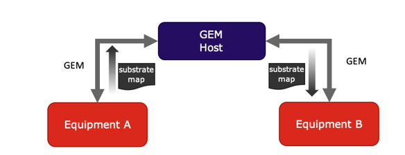
In North America, SEMI created a new task force called “Advanced Back end Factory Integration” (ABFI) to organize and facilitate this industry segment’s implementation of more robust automation capabilities. To this end, the task force is charged with defining GEM and GEM 300 support in back end equipment, including processes such as bumping, wafer test, singulation, die attach, wire bonding, packaging, marking, final test and final assembly. As its first priority, the task force has focused on updating the SEMI E142 standard (Substrate Mapping) to enhance wafer maps to report additional data necessary for single device traceability. Soon the task force will shift its focus to define GEM and GEM 300 back end use cases and adoption more clearly.

Why GEM?

GEM was selected for several reasons.

  • A lot of the equipment in the industry already have GEM interfaces.
  • GEM provides two primary forms of data collection that are suitable for all data collection applications. This includes the polling of equipment and process status information using trace reports where the factory can collect selected variables at any frequency. Additionally, collection event reports allow a factory system to subscribe to notifications of just the collection events it is interested in, and to specify what data to report with each of those collection events.
  • Most of the equipment suppliers have GEM experience either from implementing GEM on the back end equipment or from implementing GEM on their frontend equipment.
  • Factories can transfer experienced engineers from semiconductor frontend facilities into the back end with the specific goal of increasing back end automation.
  • GEM has proven its flexibility to support any type of manufacturing equipment. GEM can be implemented on any and all equipment types to support remote monitoring and control.
  • GEM is a highly efficient protocol, publishing only the data that is subscribed to in a binary format that minimizes computing and network resources.
  • GEM is self-describing. It takes very little time to connect to an equipment’s GEM interface and collect useful data.
  • GEM can be used to control the equipment, even when there are special features that must be supported. For example, it is straightforward to provide custom GEM remote commands to allow the factory to determine when periodic calibrations and cleaning should be performed to keep equipment running optimally.

Improved Overall Equipment Effectiveness Tracking

The ABFI task force has already proposed some changes to the SEMI E116 standard (Specification for Equipment Performance Tracking, or EPT). EPT is one of several standards that can be implemented on a GEM interface to provide additional standardized performance monitoring behavior beyond the GEM message set. This standard already enables reporting when equipment and modules within the equipment are IDLE, BUSY, and BLOCKED. A module might be a load port, robot, conveyor, or process chamber. When BUSY, this standard requires reporting what the equipment or module is doing. When BLOCKED, this standard requires reporting why the equipment or module is BLOCKED.

After analyzing the requirements of the back end industry segment, the task force decided to adopt and enhance the EPT standard. For example, the current EPT standard does not make any distinction between scheduled and unscheduled downtime. However, a few minor changes to E116 would allow the factory to notify the equipment when downtime is scheduled by the factory, greatly enhancing the factory’s ability to track overall equipment effectiveness and respond accordingly.

Additional Future Work

Many of the GEM 300 standards can be applied to some of the back end equipment when applicable and beneficial. The task force is defining specific functional requirements and evaluation criteria to make these determinations and publish the resulting recommendations in a new standard. Representatives from several advanced back end factories are already closely involved in this work, but more participation is always welcome. For more information, reach out to Cimetrix!

The post Semiconductor Back End Processes: Adopting GEM Judiciously appeared first on 3D InCites.

Semiconductor Back End Processes: Selective GEM300 Adoption

$
0
0

GEM and GEM300 Adoption

In a previous blog, I shared how the relatively new SEMI task force in North America called “Advanced Back End Factory Integration” (ABFI) has already decided to promote the adoption of the GEM standard. In this blog, I will explain how the task force is also planning to selectively adopt what is often called the GEM300 set of standards. I say “planning” because this is a work in progress and subject to the standardization process in which we strive for consensus among the participants. However, one can argue that this plan should not be particularly controversial since the GEM300 standards have already been adopted by several major manufacturers of semiconductor back end equipment.

What are the GEM300 Standards?

There is no official “GEM300” definition, but at a minimum, all the experts agree that the GEM300 set of SEMI standards includes the following:

SEMI Designation Standard Name
E5 Specification for SEMI Equipment Communications Standard 2 Message Content (SECS-II)
E30 Specification for the Generic Model for Communications and Control of Manufacturing Equipment (GEM)
E37 Specification for High-Speed SECS Message Services (HSMS) Generic Services
E37.1 Specification for High-Speed SECS Message Services Single Selected-Session Mode (HSMS-SS)
E39 Object Services Standard: Concepts, Behavior, and Services
E39.1 SECS-II Protocol for Object Services Standard (OSS)
E40 Standard for Processing Management
E40.1 Specification for SECS-II Support for Processing Management
E87 Specification for Carrier Management (CMS)
E87.1 Specification for SECS-II Protocol for Carrier Management (CMS)
E90 Specification for Substrate Tracking
E90.1 Specification for SECS-II Protocol for Substrate Tracking
E94 Specification for Control Job Management
E94.1 Specification for SECS-II Protocol for Control Job Management (CJM)


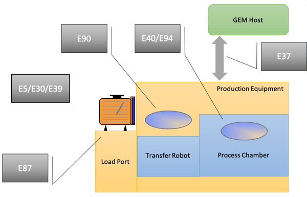
Seen together like this in a table, it seems like a lot to study and learn. And it is daunting. However, it is important to remember that most of the primary standards (like E87 and E90) also have a subordinate standard (like E87.1 and E90.1) that defines how to implement the standard using SECS-II. Although this nearly doubles the length of the list, these “.1” standards are really just extensions of the primary standard, and are all relatively short specifications. Each of these core GEM300 standards defines specifically how to use and augment the GEM standard to implement specific factory automation requirements and production operational scenarios. Basically, they work together like this:

GEM-for-Backend-2.1

SEMI E37 (High-Speed SECS Messaging Services), E5 (SECS-II) and E30 (GEM) are the core standards for any modern GEM implementation—regardless of the GEM300 additions—so of course they apply. Each of the additional GEM300 standards builds on top of E30 and E5 to define general features for data collection, alarm handling, collection event reporting and the messaging library. For example, E87 (Carrier Management) deals with the load port services, carrier delivery, and carrier removal. E90 (Substrate Tracking) reports all substrate movement from the carrier to the process chamber and any intermediate movement. E40 (Processing Management) and E94 (Control Job Management) determine which substrates to process, which recipes to use and the substrate destinations. Finally, E39 (Object Services) defines general object handling for all of the standards.

Even though the diagram shows silicon wafers—since semiconductor front end factories use this set of GEM300 standards nearly universally—their applicability goes well beyond 300mm silicon wafer processing. However, if a piece of equipment does not deal with the substrates (material) or substrate delivery directly, then it is best just implementing GEM rather than GEM300.

How can these SEMI standards be applied to other equipment?

E87 Carrier Management

Certainly, any equipment dealing with a FOUP (front opening universal pod) that holds silicon wafers can adopt E87 Carrier Management to manage the load ports and carrier validation. But E87 Carrier Management is written in a manner flexible enough that equipment handling many other types of material can adopt it. Here are the criteria:

  1. The material arrives in a container of some sort.The shape of the container, the number of slots in the container and the orientation of the slots do not matter. The container can be a rectangular tray with pockets. It can also be round with pockets. E87 Carrier Management refers to these containers as carriers
  2. The material slots in the container can be ordered.In a FOUP, the material is in a horizontally stacked orientation. However, the principles of E87 Carrier Management can also apply to other material orientations. Whatever the container type, there needs to be clearly defined slot numbering. E87 Carrier Management only defines the order for a stacked container; therefore, other container styles need standardization.

With these two criteria, E87 Carrier Management can be applied to add value to the equipment by supporting an increased level of factory automation.

What features determine whether E87 Carrier Management can be adopted?

  1. Carrier (Container) IDIf there is a carrier ID of some sort, it is of course very useful for implementing carrier ID verification. The carrier ID can be a barcode or any other type of identifier. But even if there is no carrier ID (even a barcode would suffice), then while under remote control the host can assign an ID to the carrier. Alternatively, while under local control the equipment software can generate a unique carrier ID.
  2. Carrier (Container) ID ReaderE87 Carrier Management anticipated that a unit of equipment might not have a carrier ID reader. It also anticipated that a carrier ID reader might be out of service or defective, and therefore should be ignored. Not having a carrier ID reader means that you will not have the benefit of verifying that the correct container has arrived.
  3. Number of Slots in the ContainerA standard FOUP for silicon wafers has 25 slots. But the number of slots in a container is not limited or restricted.

When can’t E87 Carrier Management be applied?

For E87 Carrier Management to be applied, the material needs to arrive and/or depart in some sort of container. If material arrives and departs continuously without any container, such as on a conveyor, then there is no container or load port for E87 Carrier Management to manage. Of course, GEM can still be applied without E87 and the other GEM300 standards, although E90 Substrate Tracking might still be useful.

What are the benefits of using E87 Carrier Management?

E87 Carrier Management provides quite a few benefits to any equipment that can adopt it.

  • Confirmation that the correct container arrived at the equipment
  • Confirmation that the container has the expected material in its various locations
  • Reporting current load port states (e.g., occupied, ready for unloading, ready for loading)
  • Placing a load port in and out of service, such as for maintenance and repair
  • Notifying the equipment when a container will be arriving
  • Managing container storage
  • Reporting when the material from a container is nearly completed processing
  • Load port identification
  • Assigning substrate IDs

E90 Substrate Tracking

The “substrate” term is not restricted to silicon wafers, but rather applies to any type of product material. This generalization of the substrate term means that E90 Substrate Tracking can be applied to many different types of equipment.

Normally substrate tracking is considered in terms of fixed substrate locations, such as a slot in a container, a specific location in a pre-aligner, the end effector of a robot arm, or a specific process chamber. However, just like a robot for handling silicon wafers can have multiple arms for handling multiple substrates, a conveyor can be similarly modeled to have multiple substrate locations. For example, if a conveyor can hold 50 small substrates at a time, then it could be modeled with 50 substrate locations for high-precision material tracking. Doing so allows E90 to be used to track substrates even while on a conveyor. The time each substrate is placed on a conveyor can be used to deduce the order of the material on the conveyor.

E90 Substrate Tracking also provides for substrate ID verification. This is only possible when the substrates have an identification code that can be read, such as a barcode or 2D data matrix, and when the equipment has the hardware capable of reading the identification code. When both are present, substrate ID verification can allow the factory to confirm each substrate before processing, and thereby reduce scrap.

When an equipment transports and processes multiple units of material internally using any type of container, it is called batch processing. E90 Substrate Tracking also supports this method by identifying batch locations and by providing data collection features specific to batch movement.

When can’t E90 Substrate Tracking be applied?

In order to use E90 Substrate Tracking, the equipment must have at least two substrate locations and work with some type of substrate. Without these, there is no benefit in implementing E90 Substrate Tracking.

What are the benefits of using E90 Substrate Tracking?

E90 Substrate Tracking provides many benefits to any equipment that handles material.

  • Providing history of substrate movement, including timestamps for each location change
  • Substrate identification
  • Substrate location identification
  • Factory substrate verification, including the automated rejection of invalid substrates
  • Providing processing status for each substrate
  • Implementing virtual substrate tracking for lost substrates

E40 Processing Management

E40 Processing Management creates a list of materials to process and the name of the recipe to use. When using silicon wafer substrates, this list is either in the form of a carrier ID and a set of slot numbers, or a list of substrate IDs.

When can’t E40 Processing Management be applied?

If an equipment processes material continuously without having a discrete set of material that is known and identified ahead of time, you cannot apply E40 Processing Management. E40 Processing Management assumes that you have a specific set of material to process. If each substrate is simply processed as it arrives, then you are better off just using GEM’s PP-SELECT remote command to choose the correct recipe.

What are the benefits of using E40 Processing Management?

E40 Processing Management provides multiple benefits when it can be applied to an equipment:

  • Easily configure the equipment to process a specific set of material with a specific recipe. For example, 20 substrates can all be processed with the same recipe, or each with a different recipe.
  • Allows the equipment to support process tuning in which specific default settings in a selected recipe can be overwritten with new values. This is far easier than creating a proliferation of nearly identical recipes.

E94 Control Job Management

E40 Processing Management can be used in a standalone fashion but is usually implemented in conjunction with E94 Control Job Management. I recommend implementing both. Even if you don’t need all the extra features of Control Job Management, it adds very little overhead and is easy to use.

When can’t E94 Control Job Management be applied?

E94 Control Job Management cannot be used without E40 Processing Management, because its primary function is to manage the E40 process jobs. Therefore, its applicability is subject to the same criteria as E40 Processing Management.

What are the benefits of using E94 Control Job Management?

E94 Control Job Management has some features that benefit some equipment:

  • Allows material to arrive in one container and depart in another. This is beneficial when the source container needs to be kept uncontaminated by the effects of a process.
  • Allows material to be sorted based on some criteria. This is beneficial when sorting takes place based on inspection and/or other conditions, and the material is subsequently routed to different destination containers based on the sorting.
  • Manages a set of process jobs. For example, one can abort, pause or resume all process jobs.

How does all of this apply to the back end industry segment?

Factories must decide if they want the benefits of GEM300. Although E90 Substrate Tracking can be applied to most equipment, E87 Carrier Management, E40 Processing Management and E94 Control Job Management are only applicable to the equipment that deliver and/or remove material in containers. The features of each standard may not seem remarkable in and of themselves, but it is important to remember that these features have been implemented in a standardized way that many equipment manufacturers and their factory customers around the world have all agreed to follow—and that is truly remarkable.

One of the primary benefits of the GEM300 standards is the factory’s ability to move material to the equipment and process it in any order. The term “process” is used very loosely with the understanding that in addition to material transformation, inspection, metrology, sorting, testing, packaging, and other manufacturing activities are all types of processing. The material can be moved from any equipment to any equipment. This flexibility is a key to the success of modern integrated circuit manufacturing. It allows for the fabrication of many products without moving equipment or setting up conveyors. It allows process steps to be added or removed at any time. It enables the optimum use of inspection and metrology equipment since the same equipment can be used before and after any process step. The GEM300 standards directly support this flexibility.

The SEMI Advanced Back End Factory Integration task force plans to standardize the criteria for determining which standards apply based on an equipment’s functionality. What I’ve explained in this posting is just the starting point for this work—there is much more to be done. We welcome more participants on the task force to ensure the standardization is done accurately and efficiently.

To find out more, contact Cimetrix at any time.

The post Semiconductor Back End Processes: Selective GEM300 Adoption appeared first on 3D InCites.

Semiconductor Backend Processes: Additional SEMI Standards Related to GEM

$
0
0

Background

In a few previous blogs, I shared how the relatively new SEMI Advanced Backend Factory Integration (ABFI) task force in North America has already decided to promote the adoption of the GEM standard and selective adoption of the GEM300 equipment communication standards. In this blog I will summarize the task force’s plans to consider adoption of additional SEMI information and control standards that are complementary to GEM and GEM300.

Additional SEMI Standards for the Backend Consideration

Many of the standards listed below were developed a few years after GEM300 but are now considered to be part of the modern GEM300 set.

SEMI Designation Standard Name
E84 Specification for Enhanced Carrier Handoff Parallel I/O Interface
E116 Specification for Equipment Performance Tracking
E116.1 Specification for SECS-II Protocol for Equipment Performance Tracking (EPT)
E142 Specification for Substrate Mapping
E142.1 Specification for XML Schema for Substrate Mapping
E142.2 Specification for SECS-II Protocol for Substrate Mapping
E148 Specification for Time Synchronization and Definition of the TS-Clock Object
E157 Specification for Module Process Tracking
E172 Specification for SECS Equipment Data Dictionary (SEDD)
E173 Specification for XML SECS-II Message Notation (SMN)


E84 Carrier Handoff

E84 Carrier Handoff is the only standard in this list that not a GEM standard because it deals with a separate parallel I/O interface. This interface is completely independent of GEM, although it is coordinated with E87 Carrier Management when both are supported. However, since E84 Carrier Handoff is often included in the GEM300 discussions and requirements, it is worth discussing here because it is a standard that the Backend industry should selectively adopt.

GEM-Backend-2-1

The E84 standard defines the handshake signals for use in a parallel I/O (PIO) interface to automate carrier delivery and carrier removal. The automated material handling system (AMHS) might use either an automated guided vehicle (AGV) or overhead transport (OHT) system, yet either way, the material is delivered in a carrier. E84 is widely used and accepted in every semiconductor wafer fab (front end) and an obvious choice for backend manufacturing when delivering carriers.

E116 Specification for Equipment Performance Tracking

E116 Equipment Performance Tracking was discussed in an earlier blog since there are plans to update this specification to better support backend operations. E116 is applicable to any manufacturing equipment in any industry because it is largely based on SEMI E10 principles which define generic terms for measuring any equipment’s reliability, availability and maintainability. As a bonus, each major component in the equipment can also be modeled to track its productivity.

E142 Specification for Substrate Mapping

E142 Substrate Mapping and its subordinate standards (E142.1 XML Schema for Substrate Mapping and E142.2 SECS-II Protocol for Substrate Mapping) define generic substrate maps and how to transfer them to and from an equipment through a GEM interface. Substrate maps are two-dimensional arrays of data that correspond to a physical substrate—which may be a wafer, strip or tray. The map defines the dimensions of the substrate, significant locations on the substrate, and can include data about the locations (such as a numbering scheme for unambiguously identifying specific locations). For example, E142 can be used to tag “known good” devices on a substrate.

Some equipment types require a substrate map before processing can proceed. Some equipment can generate substrate maps. And some equipment both require a substrate map before processing and generate an updated substrate map after processing is completed. In E142, the substrate map is expressed in an XML file that conforms with the E142 XML schema. A lot of backend equipment need substrate maps for normal operation, so E142 is an obvious choice. Note that E142 is currently undergoing some interesting improvements via the ABFI task force to store additional data needed to address enhanced traceability requirements.

Substrate mapping is an excellent demonstration of horizontal communication implemented using GEM. Horizontal communication is when data is shared directly from one equipment to another equipment. Traditionally, horizontal communication in GEM is implemented indirectly; one equipment passes data to the host and then the host passes that data on to the equipment that needs it. In this sense, the GEM host acts as a type of broker between units of equipment.

There are significant advantages in using this indirect style of horizontal communication. For example, Equipment A might inspect a substrate, generate a substrate map and send it to the host. Equipment B might later request the substrate map from the host.

GEM-backend-2-2The benefit of using a GEM host between the equipment to realize this use case is that both Equipment A and Equipment B are only required to implement GEM—which they should be doing anyway. The equipment are not required to support additional protocols and/or custom message sequences, or to be tested against specific equipment interfaces. If each equipment follows the GEM standard, they can all be integrated into the factory system and share data through the GEM host.

E148 Specification for Time Synchronization and Definition of the TS-Clock Object

A lot of data collected in the factory is only useful when properly timestamped. Moreover, timestamps can only be compared among data from multiple sources when those timestamps are synchronized. This is where SEMI E148 enters the picture.

The E148 Time Synchronization specification requires equipment to support the industry standard Network Time Protocol (NTP) and share information about its implementation. And NTP software synchronizes computer clocks.

Because the backend industry segment is trending towards more and more data collection, it is critical to have proper timestamping for that data, and therefore time synchronization for its sources. A full E148 implementation may not be required, but certainly, the equipment should support NTP as described in E148. If an equipment control system is composed of multiple computers, E148 states that they should all be synchronized with a single computer designated as the master, which is a good idea if the other computers are generating data with timestamps.

E157 Specification for Module Process Tracking

E157 Module Process Tracking does not apply to all backend equipment. To use E157 Module Process Tracking, there must be at least one process module (aka a process chamber) which processes one substrate or a batch of material at a time. If multiple substrates are processed at a time but each having different start and stop times, then this specification cannot be applied.

E157 Module Process Tracking defines a very simple processing state model which is implemented independently for each process chamber.

GEM-backend-2-3The state model reports when the process chamber is either idle (Not Executing) or processing a recipe (Executing). And when processing a recipe, each time an individual step in the recipe starts, completes, or fails, this is reported. It is up to the implementer to decide what constitutes a recipe step. In my experience, most equipment that could adopt E157 have already implemented something very similar using a set of GEM events. However, rather than implementing something custom, it is better for end-users and equipment manufacturers alike if the implementations are standardized.

E157 is a prime example of an exceptionally simple and well-written standard built on top of GEM technology that is easy to implement and provides a lot of end-user value. Hopefully the ABFI task force can develop something based on E157 principles that is well suited for backend equipment that cannot accommodate the full scope of the current standard.

E172 Specification for SECS Equipment Data Dictionary (SEDD)

Go back in time (not that far, actually), and “GEM documentation” meant a stack of printed documentation on paper that was expected to be delivered with the equipment. Today “GEM documentation” means an MS Word document, PDF file, Excel spreadsheet, or some other electronic representation of the same information. Nearly any digital format is acceptable.

Nevertheless, E172 SECS Equipment Data Dictionary is the future of GEM documentation. The GEM documentation is provided in a standardized electronic XML format called an SEDD file. E172 defines a standard XML schema. The initial version of this schema included only basic information about a GEM interface. This was expanded in a later version to include several more details. Soon, I hope to report that the E30 GEM standard has been modified to officially include SEDD files as one form of documentation. Additionally, this should include enhancing the GEM standard to allow an SEDD file to be transferred directly through the GEM interface. This will significantly improve GEM’s plug-and-play capability by enabling factory host software to consume an SEDD file and automatically configure the GEM host software to support an equipment’s specific implementation of GEM and GEM messages.

As the backend industry segment is increasingly implementing GEM in its factories, I expect SEDD files to be required from all backend equipment manufacturers.

E173 Specification for XML SECS-II Message Notation (SMN)

In order to diagnose problems in a GEM interface, it is essential to have logging for the GEM messages transferred between the host and equipment. Typically, both the GEM host and equipment’s GEM interface will provide logging functionality. In the past, a notation called SML (SECS Message Language) was used for logging GEM messages. Unfortunately, SML was never standardized or even sufficiently well defined. As result, there are many different variations of SML throughout the world. While SML notation itself is relatively easy to generate with software, the breadth of implementation variations makes it difficult to automatically parse and use.

Fortunately, the SEMI North America GEM300 task force created E173 XML SECS-II Message Notation (SMN) to solve this problem. SMN defines an XML schema that anyone can use to document and log GEM SECS-II messages. The schema is feature-rich allowing for both minimum and elaborate XML decoration. As an example of its usefulness and flexibility, the E172 SEDD schema references the SMN schema file. Because SMN is based on XML, it is both very easy for software to generate and consume. There are numerous software tools and libraries available in virtually every software programming language for working with XML. Using SMN with GEM allows GEM to continue to send and receive messages in an efficient binary format, yet still enjoy the benefits of using a decorated, human-readable text notation for diagnosing issues.

I expect the ABFI task force to recommend that the backend industry segment adopt SMN in all equipment GEM interfaces.

Conclusion

As backend factories adopt GEM, we expect that they will also want to use the latest technologies with it, including SMN, SEDD, Module Process Tracking and Equipment Performance Tracking. Watch for more details and updates from the SEMI Advanced Backend Factory Integration task force as its work progresses—and feel free to join this initiative if you want to help steer and accelerate this activity!

To download the GEM300 White Paper, click below

GEM300

The post Semiconductor Backend Processes: Additional SEMI Standards Related to GEM appeared first on 3D InCites.

FCC-approved BLE and LoRa module includes Antenna in Package

$
0
0

In engineering school, I learned that different laws of physics apply when the widely used electricity with 50/60 Hertz gets into the Gigahertz or even Terahertz range. In the decades since, I have managed to keep a safe distance to this challenging world of radio frequencies (RF) needed for transmitting data wirelessly. With Antenna in Package (AiP) becoming an important topic for advanced packaging, my luck ran finally out. I now find myself studying again RF physics: Insertion loss, modulators, mixers, S-parameter models, impedance matching, attenuators, types and characteristics of filters, etc. – so I can better understand the challenges as well as benefits of AiP for higher levels of integration.

The Evolution Toward Antenna in Package

At the June 17 MEPTEC & iMAPS webinar, Chris Barratt, the co-founder and CTO at Insight SiP, located in Southern France, described their evolution towards AiP (Figure 1). He demonstrated his many years of RF experience, outlined the strengths of the Insight SiP team – pictured above – and explained how easy their FCC approved modules make it to transmit data wirelessly. As a backbone of his presentation and example for their products, Barratt used one of their RF modules, the ISP4520. It’s designed for Bluetooth Low Energy (BLE) and Long Range (LoRa) signaling. The integrated antenna supports 2.4 GHz for BLE, 915 MHz for LoRa and is small enough to fit into the 9.8 x 7.2 x 1.7 mm package.

Antenna in Package

Figure 1: Evolution towards Antenna in Package (AiP) at Insight SiP (Source: Chris Barratt, CTO Insight SiP)

Benefits of Using RF modules with Integrated Antennas

As Figure 1 shows, modules with integrated antennas reduce a system’s form factor significantly. The shorter interconnections and lower drive I/Os in a module reduces power consumption and extend battery life. Modules with integrated antennas, like the one discussed here, also enable system design experts to quickly incorporate wireless signaling into their systems – reducing system design time and risk. Depending on the country and regulatory agency (e.g. FCC in the U.S.), every radio has to pass a more or less stringent certification process, before the entire system can be operated in their region. RF modules are either fully or mostly pre-certified and eliminate or minimize such time-consuming and costly certification efforts. Last, but not least, modules reduce the number of components on a system’s bill of materials (BOM), simplifying supply, and inventory challenges.

ISP 4520 Block diagram

Antenna in Package

Figure 2: Block diagram of the ISP 4520 module. (Source: Chris Barratt, CTO Insight SiP)

Figure 2 shows a block diagram with the functions inside baseband SoC and RF transceiver. In addition to the two packaged and fully tested ICs, this figure also shows that a significant number of other parts are needed to complete the module. In response to a question from the audience, Barratt emphasized that he prefers to use fully packaged ICs in a module, because exhaustive testing of bare dice, especially if they contain RF functions, is not (yet) sophisticated enough.

RF Module Design and Verification Flow

Barrett first described the schematic to the layout design process, then extraction and the verification steps. His team uses Altium Designer, Cadence’ Allegro SiP, or Expedition, from Mentor, a Siemens Business, for the design steps. For 3D parasitic extraction, they use Ansys’ HFSS, CST Studio, or ADS’ FEM. They create n-port S-parameter models and feed them, together with the annotated schematics and the models of baseband SoC and RF transceiver, into the Keysight ADS simulator. Then Barrett’s team simulates accurately the interactions between the two ICs, the passive components, the antenna as well as the impact of substrate characteristics on the RF signals. Insight SiP typically uses BT as substrate material. Barrett emphasized: Since using Electronic Design Automation (EDA) tools extensively, they can optimize and verify designs much faster, easier, and more accurately than with traditional prototyping. Also, EDA tools enable them to consider component tolerances, materials characteristics as well as manufacturing variations, to improve manufacturing yields, and performance of their products.

Antenna Integration Challenges

The wavelength of a 915 MHz LoRa signal is 32 cm and a quarter of the wavelength (minimum length the antenna should have) is 8 cm. A 2.4Ghz Bluetooth signal has a wavelength of 12 cm and a ¼ wave is 3cm. Considering that the entire module is less than 1 cm long, it takes RF expertise to “extend electrically” the length of an integrated, in this case, dual-purpose antenna, to meet signal transmission and reception criteria. Figure 3 gives a hint of how extending the length of an antenna works, to fit it into a small package. It also shows the keep-out zone required near an antenna.

Figure 3: Layout of an Antenna in Package (AiP) (Source: Chris Barratt, CTO Insight SiP)

Personal comments

Barrett’s presentation gave a perfect example of the benefits of higher levels of integration. While combining packaged ICs in a module is widely used today, Insight SiP’s extensive use of EDA tools surprised me. Their reasons for not using bare dice confirm what I heard from other designers: Wafer-probe needs to improve further! In addition, SoC dice designers need to include more probe pads, loop-back circuitry, built-in self-test (BIST), and even redundant circuitry, to make it easier for manufacturers to achieve high yielding multi-die ICs.

The value of the Internet of Things (IoT) depends significantly on the amount of data the low-power IoT edge nodes can capture and transmit to the cloud, using BLE, WiFi, LoRa, 5G or other standards. As the use of 5G is taking off in mobile phones, RF experts tell me that multiple RF modules, with AiP, will be needed per phone. Phase 1 of 5G deployment, using sub 6 GHz signaling, is ongoing and doesn’t require many changes to the RF modules. However, phase 2 uses Millimeter-wave signaling, will demand big changes, e.g. accurate data about existing materials characteristics at 60+ GHz and new materials that minimize insertion loss at such frequencies.

What MEPTEC & iMAPS Offer Now and Next

If you want to learn more about Barrett’s presentation, you can download his slides and/or listen to the entire presentation, as well as many previous webcasts, here.

On July 1, Stephen M. Rothrock from ATREG will address the U.S. – China trade war. Register here.

On July 15, Jan Vardaman will give her annual IC Packaging update

For Sept 16 the Known-good-die (KGD) workshop is planned. See more about it here. ~Herb

The post FCC-approved BLE and LoRa module includes Antenna in Package appeared first on 3D InCites.
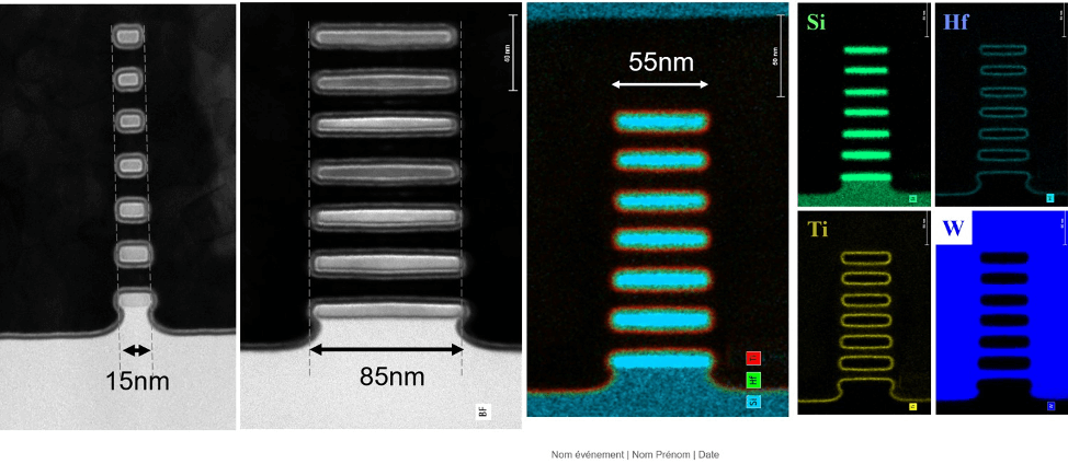
VLSI 2020: 3D Continues to Dominate Advanced Semiconductor Technology

$
0
0

As a process geek, The Symposia on VLSI Technology and Circuits has long been one of my favorite conferences. The fact that it rotates between Kyoto and Honolulu adds a bit to its attractiveness. However, VLSI 2020, as with most, was held virtually.

Having attended a reasonable share of conferences and presentations this year, I think the IEEE and the VLSI committee did a great job of making this conference available to the attendees, as well as managing the number of speakers and keeping the conference running seamlessly, or at least it seemed that way to me. As a virtual conference, VLSI added a few features that I thought helped attendees get the most out of it and possibly attend some sessions that they may not have if they have attended in person.

One aspect that I particularly like was the executive sessions that the VLSI committee included. These sessions gave a quick two-minute overview, with essentially a live Q&A session, either by the moderators of the session or via online chat. This allowed attendees to get a quick view of the session, get their questions answered, and then decide if they wanted to hear the entire paper.

Moore’s Law Continues in 3D

The advanced CMOS Si session discussed the transistors of the future. Currently, FinFETs are considered to be the transistor of choice through the 5nm technology node. Past 5nm it appears the transistor of choice will move to stacked nanosheets. TSMC and CEA-Leti presented on nanosheet gate all around (GAA). It was a bit surprising that there were only two papers on this topic, and that none of the other logic manufacturers or research groups contributed to it. CEA-Leti presented on a 7-layer GAA structure (Figure 1). Sometimes the lack of industry papers means that they are getting close to high volume manufacturing and they don’t want to tip their hand as to what they are doing.

VLSI 2020

Figure 1. 7 Layer Nanosheet structure by CEA-Leti (Source CEA Leti)

The 7-layer GAA will lead to sub 5nm technology nodes with transistors that have improved gate control and higher DC performance over FinFETs, according to the author Sylvain Barraud. The complexity of processing the GAA nanosheets is complex, so it will be a few more years before this technology is in mainstream production.

One of the possible alternatives, or it might be better to say the evolution of nanosheets, are monolithic transistors. In Figure 2, the IMEC paper presented by Sujith Subramanian demonstrates the transition from nanosheet transistors to forksheet to complementary transistors (CFETs), where the NMOS nanosheet FET is stacked on top of the PMOS FinFET. The argument is that the stacked transistors will significantly reduce the area needed for future technology nodes, thus enabling the continuation of “Moore’s Law” increasing the number of transistors per unit area.

VLSI 2020

Figure 2 Technology pathway for Logic Transistors. (Source IEEE 2020 Symposia on VLSI Technology and Circuits.)

The electrical data looks promising, but the authors have yet to build the entire 3D device. There is the PFET data and the NFET data, but no CFET data; so there is the possibility that the thermal processing of the NFET might have some effect on the PFET. A great deal of work is still needed before this will get to high volume manufacturing, but work by CEA-LETI and IMEC in this space are showing a great deal of promise.

One of the process areas that amazes me in the monolithic 3D integration is the advances in low-temperature epitaxy without anneal. Getting decent device characteristics with epi grown at 525°C is mind-boggling to this old batch epi person. Some subsequent monolithic papers that use laser annealing processes for doping and material annealing suggest that monolithic manufacturing will be mainstream relatively soon, as laser annealing enables the process flow to manage the thermal budget, such that there is little if any damage to the base device, as presented in the CEA-Leti paper on building sequential CMOS devices at 525°C or less. The low-temperature process techniques have opened the door to combining GaN transistors with silicon transistors, as shown by Intel, which can be advantageous in the power semiconductor, and communications devices as demonstrated in the Intel paper using a layer transfer technique for the Si layer on top of GaN transistors. Low-temperature processes were then used to manufacture the Si transistor with no impact on the GaN transistors.

In the distant future, once 3D integration gets neuromorphic compute under control, quantum computing or qubits will enter high-performance computing. While quantum computing will replace some of the high-performance compute applications unless quantum computing can be developed at room temperature, the use in everyday applications such as a mobile phone is unlikely, as carrying around a bottle of liquid nitrogen isn’t really feasible.

More than Moore

3D Packaging or monolithic semiconductors are increasing in importance for both high-performance computing (HPC) in AI learning, and sensors for the IoT. The need for more computing power combined with memory is critical for reducing AI learning time and potentially reducing both the time and energy needed in the learning phase of AI.

In the sensor space, being able to successfully combine, either in package or silicon, improves the performance and can reduce the power of the sensor package. It is also possible to add some additional compute power, thus creating an integrated low power nearly stand-alone sensor system. There was considerable information on the above in the short courses. The goal or challenge is to place as much compute power with the optimum memory power in the same package for AI or HPC applications.

While there was a good deal of information on the heterogeneous packaging in the short courses there were only a few papers on the topic in the conference sessions. TSMC presented one paper in the heterogeneous integration on the HPC aspects of packaging using 7nm processors and demonstrating how to effectively deliver power to the processors and chiplet package. CEA-LETI presented on their ExaNode process for building systems for HPC applications.

As memory is key for HPC figuring out how to increase the amount of DRAM available to the logic in heterogenous packaging is key. In the 3D packaging session, the focus was on memory bandwidth as a key issue for high performance and neuromorphic computing applications. CH Tsai of TSMC presented on the company’s system-on-integrated chip (SoIC) bumping process that will eventually allow for 16 DRAM to be combined into the high bandwidth memory (HBM) stack. Nine is the current technology, and the paper presented 12 memory layers. The micro bump process reduced thermal performance by 7% and 8% respectively in the 12 and 16-layer HBM.

Norio Chujo of Hitachi presented on a bumpless build cube (BBC) wafer-on-wafer (WOW) which uses a through silicon via (TSV)-to-TSV contact eliminating the bumps completely. Chujo used a wafer-level stacking technique that created a 9-layer HBM stack. Chujo is proposed that a 32-layer stack is possible using the bumpless technique. The paper claimed that by eliminating the bumps, the capacitance was 1/20 of a conventional bumping process.

As I close, if I use the VLSI conference to help predict the direction that process technology will move in the next several years. It appears that the industry will continue to focus on smaller faster transistors to continue to facilitate a form of “Moore’s Law”. However, packaging will become increasingly important in the area of both sensors and HPC, as the packaging engineers figure out how to put the devices together in the optimum configuration as business continues to move into the digital realm.  ~ D. Freeman

The post VLSI 2020: 3D Continues to Dominate Advanced Semiconductor Technology appeared first on 3D InCites.
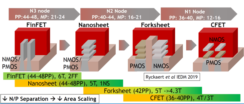

3D ICs Tear Down the Dreaded Memory Wall and Save Power

$
0
0

About 50 years ago, I started my career as a system-level designer, focused on an interface card for the Siemens T 1000. It was the first electronic teletype, destined to ship in extremely high volumes all over the world. When Siemens ramped up production, they invited me to the factory and showed me a big train car, packed up to the ceiling with my small PCB designs. Then I finally understood why my manager had pounded me almost daily with “You must reduce component and assembly cost!” This “train car impression” always encourages me to push for higher levels of integration, e.g. 2.5/3D-ICs, because they are, in my opinion, our most promising way to reduce component and assembly cost for electronic systems.

The Interface Between Memory and Processors

At the iMAPS webinar on July 1, Andy Heinig, Department Head for Efficient Electronics at the Fraunhofer Institute for Integrated Circuits (IIS) in Dresden presented a very telling example for designing cost-effective electronic systems. He showed how to increase bandwidth and power efficiency of interfaces between processors and memory – to tear down the dreaded Memory Wall. Heinig started with several slides about recent accomplishments at Fraunhofer IIS, then described Germany’s large Fraunhofer Gesellschaft, founded in 1949. Today its 74 institutes, including ISS, employ 28,000 people, the majority of them qualified scientists and engineers. See examples for some of IIS’ latest integration projects in the image above.

More Moore (Chiplets) AND More than Moore (Advanced Packaging)

50+ years of following Moore’s Law has demonstrated that higher levels of integration increase performance per Watt and allow us to pack more and more – primarily digital – functionality into a single-die IC. However, continued shrinking of feature sizes has not only increased the technical integration challenges, like development time, risk, and cost, but also the cost per transistor, and with it, has raised the cost per function.

In addition, when customers need heterogeneous functions (logic, memories, analog, RF, SERDES, MEMS, …) packed into a single-die ICs, technical capabilities and economics fail. That’s why customers are demanding that suppliers pack multiple dice (a.k.a. chiplets), all manufactured in their most suitable process technology, into an IC package. In the latest decade, multi-die IC packaging technologies have matured significantly and a growing number of system and IC designers are now relying on multi-die ICs in advanced packages, to meet specifications as well as schedules and cost targets. With multiple dice in a package, power and heat management, signal and power integrity as well as die to die interconnects are becoming more challenging. Currently, the most common way of interconnecting multiple dice is using a silicon, organic, or glass interposer (2.5D-ICs).

Heinig discussed in his presentation an example for further increasing both bandwidth and power-efficiency – while eliminating the cost of interposers to interconnect chiplets or using TSVs as signal or power paths to the PCB. Figure 2 shows Heinig’s 3D-IC stack-up.

Figure 2: System build-up: Flexible and scalable. ((Image courtesy of: Andy Heinig, Fraunhofer IIS, Dresden)

Tearing Down the dreaded Memory Wall, Demonstrated with Numbers

In addition to the the cross-section of a flexible and scalable system build-up with face-to-face, vertically stacked dice, Figure 2 shows several calculations. They assume that the large processor die interfaces directly with the attached memory dice, in the first example, via copper studs and pads. They enable 100 connections per square millimeter. At a data rate of 2 Gbits/sec   x   100 connections/mm2   x   10 mm2 interconnect area on every memory die, 2 Tbits/sec of bandwidth between the large logic die and a memory can be achieved. Figure 2 also shows in the second example that hybrid bonding, assuming a very conservative interconnect density of only 1000 connections per mm2, already increases the bandwidth to 20 Tbits/sec per memory die (assuming again 10 mm2 interconnect area).

Design tools and package assembly design kit(s) enable lower development cost/time/risk and lower unit cost.

As market pressure grows to further increase the level of integration and meet tighter schedules, achieving the demanded results with traditional prototyping becomes practically impossible. Like in the early days of ASIC technology, electronic design automation (EDA) tools are coming to the rescue. Fed with accurate data, contained in a package assembly design kit (P-ADK), like materials characteristics, package design rules, models of building blocks (a.k.a. chiplets), the EDA tools can minimize the time needed for iterations within every design step and help to optimize the die-package-board interactions.

how to tear down the memory wall

Figure 3: Block diagram of the design flow and design inputs needed. (Image courtesy of: Andy Heinig, Fraunhofer IIS, Dresden)

EDA tools also allow designers to quickly make power/performance/cost trade-offs and enable them to simulate and consider the impact of materials variations as well as manufacturing tolerances on a design’s manufacturing yield, to significantly improve it. Best of all, EDA tools can exhaustively verify functionality, timing, power dissipation and reliability of a design much faster and more accurately than a series of split-lots and/or prototypes would be able to. The block diagram of Heinig’s design and verification flow, Figure 3, shows the most important inputs needed and key design steps.

 Final Assembly on a Printed Circuit Evaluation Board

In addition to discussing the multi-die IC design, Heinig also described the validation board used in this project. Figure 4 shows an X-ray view of the multi-die design (left) a top-down view of the board (center) and a bottom view of the 3D-IC with the two memories attached (right).

Figure 4: Multiple views of 3D-IC and evaluation board. (Courtesy: Andy Heinig, Fraunhofer IIS, Dresden)

Personal Comments

Stacking logic and memory vertically (like in this design) offers the best possible bandwidth. However, for high-performance and high-power applications, the much higher operating temperature of a logic die will force a DRAM die to refresh itself frequently, reducing access time (and bandwidth) significantly. For high power and high-performance applications, the 2.5D architectures are better suited.

Heinig’s design example conveys another important benefit of 3D stacking – the significant reduction of power dissipation, due to much shorter interconnect lengths and smaller capacitances. Especially battery-power applications appreciate this benefit, that’s why the versatility and scalability of Heinig’s example architecture is a great reference for using multi-die ICs to extend battery life of handheld devices, IoT edge nodes, and other applications.

During my 40+ years in the semiconductor industry, I have introduced many new technologies and have observed every time pretty much the same behavior of the supply chain, early adopters, and mainstream users. Knowing that “history repeats itself”- here is a list of key steps and capabilities that have made and still make ASIC technology successful:

  • High-level design planning tools help to find the best architecture for the application at hand.
  • EDA design tools enable ASIC developers to manage larger and larger transistor counts, higher speeds and lower unit cost.
  • Extensive user training, e.g. educating 1000 power users/influencers created a dominant market position for an EDA tool.
  • Accurate wafer-foundry PDKs give die-developers exact guidance and tell them what’s possible and what’s not allowed.
  • Building blocks, like embedded memories, processors, data converters, etc. increase ASIC designers’ productivity.
  • Sign-off quality verification flows and clear hand-off criteria assure that a design is manufacturable and yields very well.
  • Design and manufacturing standards enable world-wide cooperation, higher efficiency, and lower cost.

Translating the proven ASIC success criteria into the Advanced Packaging ecosystem, I want to point out:

  • “Path-finding” tools will enable multi-die designers to evaluate architectures, then implement the most suitable one.
  • EDA design tools can simplify multi-die design, enable die-package-board tradeoffs, and make large designs manageable.
  • P-ADKs will give die and package designers guidance on how to best utilize assembly partners’ capabilities – at the lowest cost.
  • Education/user training, e.g. the heterogeneous integration roadmap efforts accelerate and broaden market acceptance
  • A broad range of chiplets will improve 2.5/3D-IC designers’ productivity, improve time to profit, and system reliability.
  • Sign-off quality verification flows and clear hand-off criteria will minimize iterations, save time, and engineering costs.
  • Standards across the entire supply chain will increase profitability at all steps, will accelerate market acceptance for technology innovations, and reduce time to market for every multi-die design.

Please use some of these points to discuss with your design and manufacturing partner(s) how your next (or first) integration project can best take advantage of every partner’s capabilities and contribute to your success.

On the iMAPS website, you can get all the slides Heinig used, request an MP4 file of his entire presentation, review previous presentations in this series, and register for upcoming virtual events, e.g. Laura Mirkarimi’s presentation about Xperi’s Hybrid Bonding technology.

~ Herb


The post 3D ICs Tear Down the Dreaded Memory Wall and Save Power appeared first on 3D InCites.

Virtual DAC 2020 Addresses Chiplets and Advanced Packaging

$
0
0

Why is attending Design Automation Conference (DAC 2020) important for 3D InCites readers? Two of my previous employers – National Semiconductor and VLSI Technology – could not keep up with market requirements. Lack of competitive electronic design automation (EDA) tools limited their engineers’ productivity and eventually both of these – at one point, industry-leading IC vendors – got acquired by competitors. Today’s merchant EDA tools remain essential for designing single-die SoCs and are now also becoming very important for creating multi-die ICs and (sub)system solutions in advanced packaging. Organizers of DAC 2020 recognized this, and have selected speakers who will address these concerns.

Introduction to Virtual DAC 2020

The (DAC 2020) will be held virtually from July 20-24, 2020 and offers great opportunities to check – from the convenience of your work/home-office – how EDA tools can assist you and your teams to bring cost-competitive and feature-rich IC designs to market faster. This matrix gives you an overview of what DAC 2020 has to offer, from Monday to Friday.

Keynotes and Sky Talks

If you are interested in executive-level messages about our industry, please check the keynotes, starting Monday to Thursday at 9.20 am and the Sky Talks, which take place Monday – Thursday at 12.30 pm.

Advanced Packaging Events I recommend Specifically:

On Monday afternoon check out Tutorial 10, Parts 1 and 2, organized by Farhang Yazdani from Broadpak. Six advanced packaging experts, from Cadence, Intel, Marvell, Blue Cheetah Analog Design, Broadpak, and zGlue will present and discuss chiplet integration, specifically tools, methodologies, and infrastructure required to make this very innovative way of extending Moore’s Law with advanced packaging successful.

Also related to packaging, on Wednesday afternoon check out Next-generation On-chip and In-package networks. Several speakers from AMD, GeorgiaTech, and other universities will present their far-reaching perspectives about advanced packaging, e.g. how thousands of cores will be connected, and how photonics, 3D, and reconfigurable networks will impact the future.

On Thursday afternoon you can view Will die-to-die interface IP enable chiplet-based architectures to finally achieve market success? Bapi Vinnakota, from Open Compute Project Foundation, Andy Heinig from Fraunhofer IIS, and Tony Pialis from AlphaWave IP Corp will present how high speed and power-efficient interface IP can and will contribute to the success of chiplets and advanced packaging.

Conclusion

DAC 2020, the EDA industry’s main conference offers many more topics interesting and relevant for Advanced Packaging experts. Please use the pointers above to select the topics most useful for you and your company’s success.

Also, keep in mind that Semicon West is scheduled in parallel with DAC and see SEMI’s and Francoise’s recommendations.

~ Herb


The post Virtual DAC 2020 Addresses Chiplets and Advanced Packaging appeared first on 3D InCites.

Semiconductor Back End Processes: Selective GEM300 Adoption

$
0
0

GEM and GEM300 Adoption

In a previous blog, I shared how the relatively new SEMI task force in North America called “Advanced Back End Factory Integration” (ABFI) has already decided to promote the adoption of the GEM standard. In this blog, I will explain how the task force is also planning to selectively adopt what is often called the GEM300 set of standards. I say “planning” because this is a work in progress and subject to the standardization process in which we strive for consensus among the participants. However, one can argue that this plan should not be particularly controversial since the GEM300 standards have already been adopted by several major manufacturers of semiconductor back end equipment.

What are the GEM300 Standards?

There is no official “GEM300” definition, but at a minimum, all the experts agree that the GEM300 set of SEMI standards includes the following:

SEMI Designation Standard Name
E5 Specification for SEMI Equipment Communications Standard 2 Message Content (SECS-II)
E30 Specification for the Generic Model for Communications and Control of Manufacturing Equipment (GEM)
E37 Specification for High-Speed SECS Message Services (HSMS) Generic Services
E37.1 Specification for High-Speed SECS Message Services Single Selected-Session Mode (HSMS-SS)
E39 Object Services Standard: Concepts, Behavior, and Services
E39.1 SECS-II Protocol for Object Services Standard (OSS)
E40 Standard for Processing Management
E40.1 Specification for SECS-II Support for Processing Management
E87 Specification for Carrier Management (CMS)
E87.1 Specification for SECS-II Protocol for Carrier Management (CMS)
E90 Specification for Substrate Tracking
E90.1 Specification for SECS-II Protocol for Substrate Tracking
E94 Specification for Control Job Management
E94.1 Specification for SECS-II Protocol for Control Job Management (CJM)


Seen together like this in a table, it seems like a lot to study and learn. And it is daunting. However, it is important to remember that most of the primary standards (like E87 and E90) also have a subordinate standard (like E87.1 and E90.1) that defines how to implement the standard using SECS-II. Although this nearly doubles the length of the list, these “.1” standards are really just extensions of the primary standard, and are all relatively short specifications. Each of these core GEM300 standards defines specifically how to use and augment the GEM standard to implement specific factory automation requirements and production operational scenarios. The diagram above shows how they work.

SEMI E37 (High-Speed SECS Messaging Services), E5 (SECS-II) and E30 (GEM) are the core standards for any modern GEM implementation—regardless of the GEM300 additions—so of course they apply. Each of the additional GEM300 standards builds on top of E30 and E5 to define general features for data collection, alarm handling, collection event reporting and the messaging library. For example, E87 (Carrier Management) deals with the load port services, carrier delivery, and carrier removal. E90 (Substrate Tracking) reports all substrate movement from the carrier to the process chamber and any intermediate movement. E40 (Processing Management) and E94 (Control Job Management) determine which substrates to process, which recipes to use and the substrate destinations. Finally, E39 (Object Services) defines general object handling for all of the standards.

Even though the diagram shows silicon wafers—since semiconductor front end factories use this set of GEM300 standards nearly universally—their applicability goes well beyond 300mm silicon wafer processing. However, if a piece of equipment does not deal with the substrates (material) or substrate delivery directly, then it is best just implementing GEM rather than GEM300.

How can these SEMI standards be applied to other equipment?

E87 Carrier Management

Certainly, any equipment dealing with a FOUP (front opening universal pod) that holds silicon wafers can adopt E87 Carrier Management to manage the load ports and carrier validation. But E87 Carrier Management is written in a manner flexible enough that equipment handling many other types of material can adopt it. Here are the criteria:

  1. The material arrives in a container of some sort.The shape of the container, the number of slots in the container and the orientation of the slots do not matter. The container can be a rectangular tray with pockets. It can also be round with pockets. E87 Carrier Management refers to these containers as carriers
  2. The material slots in the container can be ordered.In a FOUP, the material is in a horizontally stacked orientation. However, the principles of E87 Carrier Management can also apply to other material orientations. Whatever the container type, there needs to be clearly defined slot numbering. E87 Carrier Management only defines the order for a stacked container; therefore, other container styles need standardization.

With these two criteria, E87 Carrier Management can be applied to add value to the equipment by supporting an increased level of factory automation.

What features determine whether E87 Carrier Management can be adopted?

  1. Carrier (Container) IDIf there is a carrier ID of some sort, it is of course very useful for implementing carrier ID verification. The carrier ID can be a barcode or any other type of identifier. But even if there is no carrier ID (even a barcode would suffice), then while under remote control the host can assign an ID to the carrier. Alternatively, while under local control the equipment software can generate a unique carrier ID.
  2. Carrier (Container) ID ReaderE87 Carrier Management anticipated that a unit of equipment might not have a carrier ID reader. It also anticipated that a carrier ID reader might be out of service or defective, and therefore should be ignored. Not having a carrier ID reader means that you will not have the benefit of verifying that the correct container has arrived.
  3. Number of Slots in the ContainerA standard FOUP for silicon wafers has 25 slots. But the number of slots in a container is not limited or restricted.

When can’t E87 Carrier Management be applied?

For E87 Carrier Management to be applied, the material needs to arrive and/or depart in some sort of container. If material arrives and departs continuously without any container, such as on a conveyor, then there is no container or load port for E87 Carrier Management to manage. Of course, GEM can still be applied without E87 and the other GEM300 standards, although E90 Substrate Tracking might still be useful.

What are the benefits of using E87 Carrier Management?

E87 Carrier Management provides quite a few benefits to any equipment that can adopt it.

  • Confirmation that the correct container arrived at the equipment
  • Confirmation that the container has the expected material in its various locations
  • Reporting current load port states (e.g., occupied, ready for unloading, ready for loading)
  • Placing a load port in and out of service, such as for maintenance and repair
  • Notifying the equipment when a container will be arriving
  • Managing container storage
  • Reporting when the material from a container is nearly completed processing
  • Load port identification
  • Assigning substrate IDs

E90 Substrate Tracking

The “substrate” term is not restricted to silicon wafers, but rather applies to any type of product material. This generalization of the substrate term means that E90 Substrate Tracking can be applied to many different types of equipment.

Normally substrate tracking is considered in terms of fixed substrate locations, such as a slot in a container, a specific location in a pre-aligner, the end effector of a robot arm, or a specific process chamber. However, just like a robot for handling silicon wafers can have multiple arms for handling multiple substrates, a conveyor can be similarly modeled to have multiple substrate locations. For example, if a conveyor can hold 50 small substrates at a time, then it could be modeled with 50 substrate locations for high-precision material tracking. Doing so allows E90 to be used to track substrates even while on a conveyor. The time each substrate is placed on a conveyor can be used to deduce the order of the material on the conveyor.

E90 Substrate Tracking also provides for substrate ID verification. This is only possible when the substrates have an identification code that can be read, such as a barcode or 2D data matrix, and when the equipment has the hardware capable of reading the identification code. When both are present, substrate ID verification can allow the factory to confirm each substrate before processing, and thereby reduce scrap.

When an equipment transports and processes multiple units of material internally using any type of container, it is called batch processing. E90 Substrate Tracking also supports this method by identifying batch locations and by providing data collection features specific to batch movement.

When can’t E90 Substrate Tracking be applied?

In order to use E90 Substrate Tracking, the equipment must have at least two substrate locations and work with some type of substrate. Without these, there is no benefit in implementing E90 Substrate Tracking.

What are the benefits of using E90 Substrate Tracking?

E90 Substrate Tracking provides many benefits to any equipment that handles material.

  • Providing history of substrate movement, including timestamps for each location change
  • Substrate identification
  • Substrate location identification
  • Factory substrate verification, including the automated rejection of invalid substrates
  • Providing processing status for each substrate
  • Implementing virtual substrate tracking for lost substrates

E40 Processing Management

E40 Processing Management creates a list of materials to process and the name of the recipe to use. When using silicon wafer substrates, this list is either in the form of a carrier ID and a set of slot numbers, or a list of substrate IDs.

When can’t E40 Processing Management be applied?

If an equipment processes material continuously without having a discrete set of material that is known and identified ahead of time, you cannot apply E40 Processing Management. E40 Processing Management assumes that you have a specific set of material to process. If each substrate is simply processed as it arrives, then you are better off just using GEM’s PP-SELECT remote command to choose the correct recipe.

What are the benefits of using E40 Processing Management?

E40 Processing Management provides multiple benefits when it can be applied to an equipment:

  • Easily configure the equipment to process a specific set of material with a specific recipe. For example, 20 substrates can all be processed with the same recipe, or each with a different recipe.
  • Allows the equipment to support process tuning in which specific default settings in a selected recipe can be overwritten with new values. This is far easier than creating a proliferation of nearly identical recipes.

E94 Control Job Management

E40 Processing Management can be used in a standalone fashion but is usually implemented in conjunction with E94 Control Job Management. I recommend implementing both. Even if you don’t need all the extra features of Control Job Management, it adds very little overhead and is easy to use.

When can’t E94 Control Job Management be applied?

E94 Control Job Management cannot be used without E40 Processing Management, because its primary function is to manage the E40 process jobs. Therefore, its applicability is subject to the same criteria as E40 Processing Management.

What are the benefits of using E94 Control Job Management?

E94 Control Job Management has some features that benefit some equipment:

  • Allows material to arrive in one container and depart in another. This is beneficial when the source container needs to be kept uncontaminated by the effects of a process.
  • Allows material to be sorted based on some criteria. This is beneficial when sorting takes place based on inspection and/or other conditions, and the material is subsequently routed to different destination containers based on the sorting.
  • Manages a set of process jobs. For example, one can abort, pause or resume all process jobs.

How does all of this apply to the back end industry segment?

Factories must decide if they want the benefits of GEM300. Although E90 Substrate Tracking can be applied to most equipment, E87 Carrier Management, E40 Processing Management and E94 Control Job Management are only applicable to the equipment that deliver and/or remove material in containers. The features of each standard may not seem remarkable in and of themselves, but it is important to remember that these features have been implemented in a standardized way that many equipment manufacturers and their factory customers around the world have all agreed to follow—and that is truly remarkable.

One of the primary benefits of the GEM300 standards is the factory’s ability to move material to the equipment and process it in any order. The term “process” is used very loosely with the understanding that in addition to material transformation, inspection, metrology, sorting, testing, packaging, and other manufacturing activities are all types of processing. The material can be moved from any equipment to any equipment. This flexibility is a key to the success of modern integrated circuit manufacturing. It allows for the fabrication of many products without moving equipment or setting up conveyors. It allows process steps to be added or removed at any time. It enables the optimum use of inspection and metrology equipment since the same equipment can be used before and after any process step. The GEM300 standards directly support this flexibility.

The SEMI Advanced Back End Factory Integration task force plans to standardize the criteria for determining which standards apply based on an equipment’s functionality. What I’ve explained in this posting is just the starting point for this work—there is much more to be done. We welcome more participants on the task force to ensure the standardization is done accurately and efficiently.

To find out more, contact Cimetrix at any time.

The post Semiconductor Back End Processes: Selective GEM300 Adoption appeared first on 3D InCites.

Virtual SEMICON West 2020: The Soft Launch

$
0
0

Whew! That was a busy two hours! Here’s a short blog post about my initial impressions of Virtual SEMICON West 2020, the sessions I attended, and some tips for managing the next few days.

First of all, the chat function in the virtual booth is great! I had some great quick discussions, and the platform makes it easy to record and save follow up action items with the people you interact with. I can see it’s going to be a very busy week.

One tip: If you are going to attend a session, I recommend setting yourself to “do not disturb” so that you can focus on what you’re without being interrupted. I forgot to do that and found myself trying to juggle networking while watching the sessions, The Most Productive Half Century in History, and Collaborating on Innovation: The SEMI and imec Partnership.

Good Ole Boys Talking about the Good Ole Days

I’m not sure what I was expecting… it’s almost like I forgot there was a global pandemic, and everyone is working from home. So, if you too were imagining TED-esque videos, just get that image out of your mind. Also, since we did our own, “Zooming into SEMICON West” series, I should have expected the same. And that’s exactly what this session was like – a conversation between Dan Hutchison, VLSI Research, and various members of SEMI committee members reminiscing about the good old days of the semiconductor industry from the comfort of their home offices. (These guys have some really nice bookshelves.)

Jim Morgan, Steve Newberry, Dave Toole, and Stan Myers all share their memories about how SEMI began, from early days as a US organization to its shift to become an international trade association when Japan’s semiconductor industry began to thrive.

Steve talked about how “a bunch of crazy start-ups” came together to figure out how to deliver value. He talked about the struggle with scale and scope, and how vertically integrated companies needed six months lead time, and how much there was to be learned from Japan’s approach to manufacturing.

Stan talked about how some members wanted SEMI to remain an American organization, and Ken Levy and Bill Reed pushed to take it global. He said developing global standards was the highlight of SEMI’s work and brought the industry together. Jim Morgan pointed out the standards work was funded by the SEMI exhibitions.

Dan and Dave brought us through The Great Consolidation, the impact that had on SEMI trade shows, and how the character of the show has changed because of it.

One thing that stood out to me from this conversation and those who participated, was the very white maleness of the old days of SEMI. I can’t even complain that this panel isn’t diverse or inclusive, because it’s just how it was: These men are some of the key people involved SEMI from the start, remembering some of the great moments of our industry. You can check out the archived video of this presentation here yourself after 5 pm today.

Collaborating on Innovation: The SEMI and imec Partnership

The second live session I attended was a discussion with SEMI’s Ajit Manocha and imec’s Luc Van Den Hove, moderated by SEMI’s Bettina Weiss, who moderated the discussion. But according to Ajit, Bettina did a lot more than that. He credited her with (and thanked her for) putting this partnership together. So I want to personally congratulate Bettina on this successful partnership!

While SEMI and imec have enjoyed an informal partnership for years, Ajit said they have now formalized the relationship and put into the SEMI governance that imec and SEMI will always be in sync. He called imec the “powerhouse of European research.”  (I am wondering what CEA Leti, Fraunhofer, and others think about this statement…)

For his part, Luc described SEMI as “the networking organization of the industry” that is successfully grown partnerships, while the essence of imec is forming ecosystems. “Together, we can deliver more value to the industry and link to new value change.”

The two went on to discuss their viewpoints on Moore’s Law, various roadmaps, and the importance of accelerating tech in the face of the COVID-19 crisis. Rather than reveal more of the details, I’m going to encourage you to view it on-demand after 5 pm today.

Final Thoughts

I’m looking forward to seeing what Al Gore’s home office looks like tomorrow, as well as some of the other keynote speakers.

If you visited booths today and had some issues, be sure to let technical support know. Today was the soft launch to work out final kinks and bugs. If you visited our booth this morning and didn’t find your video (Namics, Cimetrix, ASE) they are all there now! Check back tomorrow. I’ll be in our booth in the afternoon daily – so stop by for a chat!


The post Virtual SEMICON West 2020: The Soft Launch appeared first on 3D InCites.

How we Helped a Customer Deliver a GEM-compliant Equipment using CCF

$
0
0

Welcome to the first posting in the Cimetrix CIMControlFramework (CCF) Services blog series! While Cimetrix has been providing professional services for many years, in order to better serve the growing demand from many new equipment maker customers worldwide that have purchased our CCF product, Cimetrix earlier this year formed a new CCF Services group, reporting directly to the CEO. Being a senior developer at Cimetrix for the past 15 years in a variety of positions, I was delighted when asked to lead this group. We have an outstanding team of software engineers highly experienced in factory automation, equipment control software and SEMI standards. We are dedicated to ensuring our customers’ success by providing training, consulting, and developing custom solutions for our CCF customers. We love learning about the myriad ways that companies can integrate CCF with their equipment to meet the material handling and factory automation requirements of their factory customers. Our goal for these articles is to share some of the lessons learned and other implementation insights to help you efficiently build manufacturing equipment that is sophisticated, robust, and productive. To this end, our first posting will deal with one of the most common requests we get – enjoy!

– Forward by Brent Forsgren, Director of CCF Services

How we helped a customer deliver GEM-compliant equipment using CCF

The Goal

One of our recent customers wanted to build a new type of LED manufacturing equipment that could be controlled by a Factory Host using the standard GEM Remote Commands: PP_SELECT (Process Program Select), START, STOP, ABORT, PAUSE and RESUME. The equipment could be delivered in a variety of physical configurations, including 1-to-multiple source cassettes for product material, and 1-to-multiple process modules. It also had multiple destination cassettes to be filled according to the post-process analysis results. The initial instance of the equipment had 4 loadports (LPs) and four process modules (PMs).

The functional requirements were clear – that was the good news. Now for the rest of the story… the project schedule and budget constraints were closing in, so we needed to work quickly and efficiently with the customer to get it done. Sound familiar?

The Approach

The Cimetrix CCF Services team always works closely with the software team of the equipment manufacturer. In this case, we started with one week of mutual discovery and in-depth hands-on training. Team members were fully engaged and picked up the CCF capabilities very quickly. This included even some of the more advanced features, such as developing a scheduler that would control the components of the customer’s application. We regularly fine-tune training modules to 1) introduce CCF concepts, 2) expose common challenges and potential approaches, and 3) provide realistic implementation practice exercises. As anticipated, the customer was able to use the results of the training exercises in the actual equipment control solution. We also kicked off the project with our work-breakdown exercise to more deeply explore the unique requirements for their specific equipment type.

After an intense first week, everyone on the project team concluded that CCF would in fact be a strong match for their needs. CCF features direct integration with our CIMConnect, CIM300, and CIMPortal connectivity products to provide full GEM, GEM300 and EDA compliance. Because the Cimetrix connectivity products are deployed in every semiconductor 300mm factory in the world, our customers can be assured that they will meet their customer’s factory automation requirements. In this application, the end customer’s LED factory only required GEM.

To address requirements that may go beyond the basic GEM standards, CCF also provides support for custom remote commands, data publication, and alarm management. Finally, CCF supports integrating custom hardware devices using CCF’s base Equipment Classes.

To prove all was working, we chose the Cimetrix EquipmentTest product to develop and execute a set of unit tests that emulate communications with the factory software using GEM messages. This was not intended to be a comprehensive set, but rather just enough to show the equipment passed round-trip system testing. In this context, round trip means showing that the equipment can move material from the incoming cassette to the aligner to the process module and back into the cassette. EquipmentTest also supports editing message settings and parameters on the fly to experiment with different configurations of a round-trip test.

The Challenge: “The Host is unavailable, but we need to validate that the equipment is both GEM compliant and accomplishes the communication flows the end user requires.”

We get this challenge a lot… Our customers almost always develop the host interface and the embedded control software in parallel and integrate them later in the project. This makes sense at one level, but it does introduce a “chicken and egg” problem for testing this kind of GEM interface. In particular, how can our customer provide evidence that the solution will work with the factory host without testing with the actual host system? Our answer: apply our EquipmentTest custom plugin capability to simulate the end user’s host so we can validate all necessary communication between host and equipment.

Our protocol validation product, EquipmentTest, makes it possible to simulate communications between an equipment control implementation and the host. And although it is impractical to implement scenarios for every possible interaction, we can create enough representative scenarios to be confident the “happy path” (i.e., no errors) will work and that the interface will handle a large handful of “sad path” cases as well.

Outcome

We passed all the tests! “Let’s go get some tacos.”

Specifically, we validated that the communications interface supported…

  • Standard GEM Remote Commands
  • Custom Remote Commands
  • Material tracking
  • Data publication

In closing, we must emphasize that our customer should take most of the credit here. Nevertheless, we enjoyed observing, consulting, and testing the equipment. It is always gratifying to see the CCF solution fit so seamlessly into the hardware, execute its commands with optimal timing, and not break anything in the process! Truly a successful, joint team effort.

If the situation above resonates with your current challenges and past experiences, give us a call. We look forward to working with your software engineering team to speed your time-to-market and deliver a high-quality solution quickly, allowing your team members to focus on developing value-added functionality for your customers.

The post How we Helped a Customer Deliver a GEM-compliant Equipment using CCF appeared first on 3D InCites.

Viewing all 2184 articles
Browse latest View live