Quantcast
Channel: 3D InCites
Viewing all 2184 articles
Browse latest View live

EV Group Completes Construction of State-of-the-Art Cleanroom Facility at Corporate Headquarters

$
0
0

Newly opened Cleanroom V building nearly doubles cleanroom capacity and strengthens capabilities of EVG’s NILPhotonics® and Heterogeneous Integration Competence Centers

EV Group (EVG), a leading supplier of wafer bonding and lithography equipment for the MEMS, nanotechnology and semiconductor markets, today announced that it has completed construction of its new Cleanroom V building at its corporate headquarters in Austria. Built from top to bottom with the latest cleanroom design and construction technology, the new building nearly doubles the cleanroom capacity at EVG’s headquarters, and will be used for product and process development, equipment demonstrations, prototyping and pilot-line production services. The Cleanroom V building, which is part of a 30 million Euro investment announced last year, will officially open in August.

EV Group’s new Cleanroom V facility nearly doubles the cleanroom capacity at EVG’s headquarters and houses a modern training center with multiple dedicated areas for customer and field engineer training.

The new Cleanroom V building is directly connected to EVG’s existing cleanroom and applications lab, and provides approximately 620 square meters of additional Class 10 cleanroom floor space. The new building also houses a modern training center with multiple dedicated areas for training customers and field service engineers on EVG equipment platforms. As part of the expansion investment, the existing cleanroom and applications lab facility have also been upgraded, including the creation of redundant systems to ensure the highest availability and new safety features.

EV Group personnel are finalizing the interior of the company’s new state-of-the-art Cleanroom V facility, which includes dedicated co-development areas. The facility will officially open in August.

Enhancing EVG’s centers of technology excellence

The added capacity afforded by the new Cleanroom V building will strengthen the capabilities of EVG’s NILPhotonics® Competence Center and Heterogeneous Integration Competence Center™, which provide world-class process development services, and serve as open access innovation incubators for customers and partners across the microelectronics supply chain. Through these centers of technology excellence, EVG helps customers to accelerate technology development, minimize risk, and develop differentiating technologies and products through the implementation of nanoimprint lithography and heterogeneous integration, respectively, while guaranteeing the highest IP protection standards that are required for working on pre-release products.

“We are extremely proud of the technical innovation and know-how that went into the construction of this new cleanroom. It is truly a world-class, state-of-the-art facility down to the smallest details—arguably on par with some of the most technically advanced cleanrooms in Europe,” stated Markus Wimplinger, corporate technology development & IP director at EV Group. “For EVG, this new facility will greatly enhance our ability to co-develop future applications and technologies with our customers. In particular, we see it benefiting our competence centers, which have seen particularly strong activity and demand. The unique services offered at our NILPhotonics and Heterogeneous Integration Competence Centers enable our customers and partners to shorten development cycles and create novel products in these critical application areas.”

Behind-the-scenes look at the advanced sub-fab of EV Group’s Cleanroom V facility, which has been designed with redundant systems to ensure the highest availability and new safety features.

With its technology competence centers and strong customer partnerships, EVG is uniquely positioned to provide uninterrupted process development services and support for its customers. At the same time, EVG’s local installation and support teams as well as remote support capabilities enable continuous installation and service operations of EVG’s equipment. For more information on EVG’s services, please visit: https://www.evgroup.com/services/.

For more information on EVG’s NILPhotonics Competence Center and Heterogeneous Integration Competence Center, please visit: https://www.evgroup.com/products/process-services/.

EVG will showcase its complete suite of wafer bonding, lithography and resist processing solutions at SEMICON West, to be held virtually this year on July 20-23. Attendees interested in learning more can visit our virtual booth and arrange a live chat with an EVG representative or download our latest product information.

The post EV Group Completes Construction of State-of-the-Art Cleanroom Facility at Corporate Headquarters appeared first on 3D InCites.


COVID 19 and Black Lives Matter Change the Conversation for SEMICON West Keynotes

$
0
0

I had a dream last night that the SEMI team was a little upset with me because we were getting more visitors to our booth to watch the Zooming into SEMICON West interviews than they were getting for the live keynotes. Wishful thinking, I know. But I thought I’d put it out there. (Seriously – go check them out. They’re a lot of fun.)

This morning, I took my own advice and set my status to “do not disturb” so I could focus on some of the live SEMICON West keynotes and panel discussions. As this virtual experience unfolds, I feel like there is a lot to unpack and share. What do I think of the format? What do I think of what was said? Why did I come up with this particular title? Let’s start with these and see how far we get.

SEMI Has a Sense of Humor

Let’s remember, this was supposed to be a celebration of epic proportions. After all, this is SEMI’s 50th anniversary. Live SEMICON West was in the works for a year. 2020 was going to be a big comeback year for the industry. The decision to abandon those plans, take this event virtual, and find a way to make it a celebration shows character. It was one of those laugh or cry moments, and SEMI chose to laugh. Check out Dave Anderson’s welcome address to find out what I mean (once the recorded version is available).

For their parts, Ajit Manocha and Bertrand Loy set an even more positive tone. Despite the fact that we are in the midst of a global pandemic, increased trade tensions, and other uncertainties, they reported that the semiconductor industry is following a growth trajectory for the second half of 2020 and that 2020 will see even more growth.

“This industry is vital to solving the uncertainties surrounding us,” said Manocha. “We haven’t felt the impact as much as other (industries), and we expect to see growth. Some of the old timers say they wish they were just starting out now, as we grapple multiple tsunamis to arrive even stronger.”

Loy applauded SEMI for “shifting priorities to help the industry effectively navigate these challenges” by aggregating best practices for resources and providing guidance for emerging trade issues. He said he’s feeling a spirit of solidarity, and that the transition to Virtual SEMICON West that had to be done in short order demonstrates the resourcefulness of the industry. “It’s nothing short of amazing,” he said. “I don’t believe there is a better way to celebrate 50 years than to reaffirm our purpose.”

Where am I Sitting Right Now?

Here’s where I am right now.

Dave Anderson reminisced for a bit about the very first SEMICON West in 1970 that took place in the San Mateo fairgrounds. Meetings took place in rented RVs and exhibits were set up on the racetrack. Attendance was at 50% capacity the first year, but by 1974 was a sold-out show. He recalls the “general excitement about being involved in something that set out to change the world.” And now the world has changed in six months, and the same innovative spirit was put to work to create this virtual event. He asked us to take a moment and look at “where you’re sitting right now” comparing this experience with something right out of the Jetsons.

Where I am right now is at my laptop in my family room, where I’ve been working for the past six months. And it feels strange to be watching these events here rather than in the Yerba Buena auditorium at the Moscone, snapping photos with my smartphone and tweeting out bits and pieces. Instead, I’m grabbing screenshots and hopping back and forth between the virtual booth and sessions. I’m certainly not getting my steps in, and I’m bummed that I don’t have the annual Kiterocket party to look forward to tonight. (However, in keeping with the tradition of SEMICON West Day 1, I was slightly hungover when I logged in this morning… just saying.)

SEMICON West Keynotes: Conversation with Al Gore

As I mentioned in my preview post, Al Gore’s featured keynote discussion with Green.Biz’s Heather Clancy is one thing that didn’t change from a live to a virtual format. But I do wonder how differently his remarks would have been if been had the pandemic and Black Lives Matter (BLM) protests had not happened in the first half of 2020. I’m guessing the climate change and sustainable manufacturing conversation would have been the same, but I doubt they would have been linked to COVID and BLM. And thus, the inspiration for my title.

“The pandemic reminds us that when scientists are warning us in dire terms, it’s best not to ignore them. We were warned about this and we should have listened,” Gore said. “Climate scientists have been warning us for even longer about using the atmosphere like a sewer.”  He added that BLM reminded us so powerfully of the problems with racism around the world and that it’s a good time to focus on warnings we should heed. (The connection between the pandemic, BLM, climate change, and the semiconductor industry was still not clear to me, but we’ll get there. I promise. Read on.)

He also said that while the pandemic crisis can be measured in months, the climate crisis is measured in centuries. He shared sobering numbers like:

  • 19 of the last 20 hottest years occurred in the past 20 years
  • We are still putting 150M tons of carbon emissions into the atmosphere every 24 hours

But he’s hopeful because he says we are in the midst of a sustainability revolution, powered by artificial intelligence (AI) and other technological advancements. Global investment in renewables last year was 3X that of fossil fuels. Electric vehicles are advancing, and the cost is coming down. 44 governments around the world are requiring the phase-out of internal combustion engines.

He also noted that the climate crisis offers the opportunity to create tens of millions of new jobs, citing solar installers and wind turbine technicians as the two fast-growing.” This can be the stimulus we need for sustainable prosperity in the wake of the pandemic.” he said.

Gore told Clancy that he didn’t want to discuss politics because he’s “a recovering politician and doesn’t want to relapse.” But he did share some of his realizations about COVID and the BLM movement:

  • There is a direct correlation between the burning of fossil fuels and the mortality rate of COVID 19
  • The reduction in travel and work-from-home situation that has caused us to shift to virtual interactions is showing us that it works well, and maybe we don’t have to fly so much
  • There is a privilege associated with having “Zoomable” jobs and it is coming to the forefront
  • It takes 11.5 black families to make up the average income of one white family

An awakening is taking place, he said, and the younger generation is demanding a better future, and they would be excited to know what this industry has planned to take us there. He talked about the advantages of diversity and inclusion, as well as a democratic approach to making collective decisions.

And as wonderful as semiconductor technology and the things it enables are, the reality is we have a massive carbon footprint, due to the amount of electricity required to build everything from chips, to the equipment needed to make them, as well as the power the data centers needed to support the applications that use them.

Lastly, Gore talked about environmental justice, and how climate change has an impact on communities of color. How can semiconductor industry help? He pointed out, and rightly so, that the tech industry has work to do to deal with the struggle to become more racially and culturally diverse. Software companies have been broadening hiring funnels. This could be increased in the semiconductor industry.

Gore implored us to work together to reduce our carbon footprint and decarbonize data center power, increase diversity and inclusion in our companies.

An Industry Rises to the Challenge

In doing so, he set a perfect stage for both Garry Dickerson’s keynote and the Executive panel discussion on enabling sustainable growth of AI, data centers, and cloud computing.

Dickerson outlined all the measures Applied Materials in committing to address all these issues, while still driving the technology roadmap.

He stressed the company’s commitment to a sustainable future and said it is irresponsible to double or triple environmental impact while double or tripling growth of the company. He stated the company’s commitment convert to 100% renewable energy by 2022 in its US operations, and 100 globally by 2030.

SEMICON West Keynotes and panels

Applied Materials’ commitment to sustainability.

Dickerson also noted that the BLM movement was a wakeup call. “We are stronger when we stand together against discrimination,” he said. He talked about Applied’s plan for transparency and publishing representation data. “We are committed to bringing more women and under-represented minorities to all levels,” he said.

The executive panel was probably the most interesting session of the morning. Representatives from ARM, Google, Microsoft, and VMware shared ideas and approaches to reduce the carbon footprint of data centers, and how AI can help.

SEMICON West Keynotes and Executive Panels.

Executive Panel on Bending the Climate Curve

Rob Aitkin, ARM, said the company is looking at system-level solutions implementing 3D integration approaches to reduce power needs (YEAH!). He said moving data is inefficient, so we need to bring compute closer to memory and that means die stacking or moving AI to edge.

Cliff Young, of Google, suggested we return to Denard Scaling, in which performance improves while power reduces.

Intel’s Samantha Alt says the key is to make data centers as efficient and green as possible – carbon-free or at least carbon neutral. This requires improved collaboration between manufacturing hardware and software.

Applied’s Ellie Yieh had a two-fold answer: working to make tools more efficient, and working with customers to drive performance, power, and cost (PPAC) scaling, by pushing AI closer to device and materials and vice versa.

Moe Tanabien of Microsoft focused on the advantages of AI at the edge as an important part of the energy use solution.

Nicole Piell-Moelter of VMware talked about using AI, machine learning and edge computing to integrate more renewable energy into the grid and regulate

Moderator Eric Masanet of UC Santa Barbara wrapped it up nicely, saying it’s complicated, and there’s no end in sight as the world becomes interconnected. We could see a rise in energy use if we don’t get a handle on it. On the other hand, we can also leverage semiconductor technology to bend the climate curve. But it requires a large scale commitment to address climate change. Honestly, there was a lot more to the discussion, so if you are able, I recommend putting it on your SEMICON West watch list.

Let’s Not Do That

I wouldn’t be me if I didn’t also voice my opinion on the downside of what I saw today, and that was leveraging COVID 19 as an advantage. Gary Dickerson seemed a little too excited about the opportunities afforded this industry by the pandemic. He said the world is relying on semiconductors more now than ever before, with work- and school-from-home situations. (Even if it’s true, let’s tone it down a bit.) “I’m excited about the trends,” he said. “AI and the data economy will change everything.”

Futurist Steve Brown was another one that was a little too eager about COVID 19, calling it both “a great accelerator and great defroster, forcing us to embrace digital change.” According to Brown, the pandemic presents operational challenges for business and we can help. He actually advised us to take advantage of it, because there is a “ton of investment driving technology innovation in aspects of a business.”

He noted how digital communication, such as telehealth shot through the roof since the pandemic. Yeah, Steve, because we don’t want to DIE. Most of us would still prefer to see our doctor in person.

And let’s not forget that the digital world is only available to those who can afford to participate. Nobody mentioned all the school children living in under-served communities who can’t access online school because they can’t afford a computer. Futurists always forget that technology often drives a bigger wedge between the haves and the have nots.

As always – lots of food for thought and discussion from SEMICON West keynote sessions. And with this digital platform, you’ve got 60 days to check out the recorded versions. Let’s see what tomorrow holds. And if you’re wandering around, stop in to say hi!  – FvT

PS: I was right about getting to see Gore’s home office. But I thought the bookshelves would be bigger.


The post COVID 19 and Black Lives Matter Change the Conversation for SEMICON West Keynotes appeared first on 3D InCites.

Cruising the Virtual SEMICON West Expo Hall

$
0
0

This morning at Virtual SEMICON West, I tried to attend a bunch of sessions and take notes so I could write about them. I really did. But I was experiencing information overload. And so, I decided to just listen to and watch a few, and maybe go back to the ones that really inspired me. Then I spent time cruising the SEMICON West Expo Hall to visit our community members and get their feedback on this virtual version of an iconic event.

Recommended Viewing

One of the beauties of a virtual conference is on-demand content. Here are a few presentations that I definitely want to revisit, and I suggest if you have time you watch them too.

Tel’s Terry Higashi’s talk tops my list for today. He was a breath of fresh air in a world that has become so divisive. In this time of uncertainty, he says science and technology can help by being mindful of protecting human rights, promoting health, reducing poverty, spreading education, and saving the environment. It’s about acting from a place of humanity. In the case of COVID 19, we can contribute to humanity by wearing a mask and maintaining a social distance. As an industry, we can tap into “the wisdom of collaboration.” Higashi noted the Distributed Computing Project, as an example. The DCP comprises Individually owned computers that are linked, networked, and used to analyze Covid-19 protein sequences. This leads to useful information for the treatment of the disease. He had other pearls of wisdom to offer, so be sure to check it out.

Another presentation I want to spend more time with is Paul Saffo’s talk on “Chasing Fires” by which he means chasing exponential events that if left unabated, results in catastrophic consequences – such as we’ve seen with COVID 19. Saffo is a forecaster for large-scale technology change, which I interpret like this: his job is to scare the crap out of us, so we do something before it’s too late. Not the feel-good approach of Higashi’s presentation, but effective all the same.

According to Saffo, the pandemic has been the most predicted event. And the second most predicted event in our future is a great earthquake – magnitude 8.3, that will eventually hit Silicon Valley.

Our job, as an industry, is to help overcome exponentials that are impacting the general public, he says. He says over the next five years, that means looking for consequences of an exponential, not just the opportunities it might bring to our industry. He called on us to anticipate, educate, and think about how we can change the slowest part of the exponential equation to create a world where institutions and societies respond early to exponential change. Catch it when it starts, starve it of fuel, so you can put it out early. (I think a few people in Washington would benefit from this advice.)

Onto the SEMICON West Expo Hall

I decided to spend the rest of the morning doing what I always do on Day 2 of SEMICON West – cruising the Expo Hall and visiting with 3D InCites community members to see how the show is going for them. Here’s what’s weird – I’m sitting here in my family room and I KNOW I’m in virtual chats, but in my head, the person on the other end of the chat is in a booth at the Moscone Center – not also sitting in their home office or kitchen, chatting back. Does anyone else have that feeling?

When I expressed this to EV Group’s Dave Kirsch, he remarked that was impressed with the effort behind the networking or ‘expo-experience’.  “I think Semi really tried to deliver the “meeting in the aisle experience,” he added.

For many attendees and exhibitors, attending a virtual event is new to them – especially for those who have been regulars at SEMICON West for the past 10, 20, or 50 years. The opinions people run the gamut from: “I’m still trying to figure out this platform” to “This is JUST LIKE a real show.” Or “It was slow the first day, only one lead” to “We’ve had lots of activity, but mostly overnight”.

Everyone agrees on one thing: SEMI has done a stellar job in the time they’ve had to work with when the only other responsible choice would have been to cancel SEMICON West altogether. They get high marks for researching options, pivoting on everything, and pulling it off with no time to spare. Any negative comments were not directed at SEMI, but the difference between a live and virtual show.

“It doesn’t make up for the human element of face-to-face interaction, but it is making the best of a tough situation,” noted Garrett Oakes, EV Group.

“SEMI did a great job reaching out to exhibitors and gauging next steps back in April/ May,” said Andrew Larson, CyberOptics. “The virtual experience they put on together with 6Connex is working well functionally, but It is something to get used to, in comparison to an in-person floor experience.” He added that going forward, he doesn’t think virtual shows will ever fully replace events, but maybe a hybrid of both virtual and face-to-face, with scaled-down live events, will be a viable solution.

“The platform here is nice, the challenge comes with us learning to engage people differently,” noted Ryan Honeycutt, imec. “I appreciate trade shows pivoting so quickly to provide an alternative to in-person experiences but of course it’s not as effective so far as a physical show. We will come together as a team to find some best practices going forward.”

“It’s been a good event overall and we are making some new connections, as well as saying hello to people we know,” said Mike Pinelis, Microtech Ventures.

And Chip Scale Review’s Larry Michaels shared that traffic from “the little screen” in their virtual booth, where the new Chip Scale Review website was shared, resulted in 5,547 new users, and 10,797 pageviews, without having announced they were launching a new website. That’s impressive.

“I quite like it from a presentation perspective,” said Michelle Bourke, Lam Research. “I can see more of them, and get from one to another quickly rather than racing across the different parts of Moscone/ San Francisco! I don’t like not seeing people though.”

One thing that could not be recreated virtually, and is sorely missed by me, my colleagues at Kiterocket, and several hundred invited guests, is the annual Kiterocket SEMICON West After Party, which would have taken place last night. Let’s hope that we will all be together again next July for the real thing. ~ FvT


The post Cruising the Virtual SEMICON West Expo Hall appeared first on 3D InCites.

Before SEMICON West 2020, There was IMEC ITF USA 2020

$
0
0

Each year as SEMICON West approaches, I look forward to the IMEC ITF USA event. For the past several years IMEC has been one of the kickoff events for SEMICON West.  This year was no different, IMEC just kicked things off a bit early, holding the ITF USA 2020 virtual event on July 7 instead of SEMICON week.

One of the things I enjoy about the IMEC event is that you get a good overview of the technology roadmap and what some of the brick walls, to use an old Sematech term, are and what programs IMEC has in place to address those challenges.

For those reading this post who are not familiar with IMEC, they are one of the leading semiconductor research consortiums and are based in Belgium.  IMEC typically selects a project that is pertinent to the Industry and opens an invitation for companies to join them in the research effort.  These projects have been essential in helping the semiconductor industry continue to shrink along the lines of Moore’s Law, but also have created significant “More than Moore” research projects to help the industry resolve some of the critical issues facing power and communication semiconductors.

This year’s ITF USA did not disappoint, due to the virtual nature of the event IMEC was able to include some of the projects they are working on in mini-interviews/presentations that gave the audience a good idea of what work was taking place, and giving companies the opportunity to partner with these researchers. The researchers presented in a concise manner, similar to what you would do at a trade show in the booth, you then had the opportunity to chat with the speaker to ask deeper questions.  Topics covered were AI Chip, Quantum computing, IMEC. IC-link ASIC services, Optical Beamforming, Silicon Photonics, and System-level reliability for SOC.

Yes, The Industry is Still Working on Shrinks

IMEC has had a research focus on integrated circuits, as well as on healthcare for as long as I have been associated with them, this ITF USA was no different.  Luc Van Den Hove the president and CEO of IMEC kicked things off with an overview of where the industry is headed from what is driving IC technology and what IMEC is doing to help the industry develop technology for those drivers. It all begins with the transistor and the industry being able to continue making transistors smaller faster and cheaper.  In recent years the industry has needed to address the power, performance, area, and cost (PPAC) challenges.  Since 28nm the cost to make transistors has been increasing, but the industry has managed to mitigate the cost and performance declines with new technology such as finFETs and materials to keep the performance and cost close to the original curves; however, even with the PPAC  to accomplish drivers such as analytics, AI, augmented reality, 6G, and a more seamless user device experience, smaller transistors are still needed.

So, for those that are banging the gong that “Moore’s Law is Dead”, there is still life, from a shrinking perspective, even if the PPAC does not follow the traditional curve. Sub 1nm which is a 7x shrink from today’s leading-edge production, could emerge in some pilot lines in less than 0 years.

Figure 1 Transistor density and performance trends (Source imec ITF USA 2020)

Van Den Hove laid out the transistor road map to below 1nm, and the proposed lithography road map to get there. The transistor road map moves from finFET to nanosheets, to Forksheet to CFET, to 2D materials in the Channel. The roadmap moves the industry from the current 7nm technology node down to below 1nm at a rapid pace.

Figure 2 IMEC transistor road map. (Source imec ITF USA 2020)

To reach below 1nm transistor new architecture, 2D Channel, materials, WS2 and lithography, high NA EUV, techniques will need to be developed to achieve sub 1nm technology. Van Den Hove touched on this topic and then Martin Van Den Brink of ASML presented on the progress taking place in EUV lithography.

Packaging is Critical to Achieve AI and Data Center Goals

However, to successfully meet the performance needs of AI, neuromorphic computing, and to reduce the energy consumption required for AI learning systems, significant changes to the layout of logic and memory are needed.  Today’s systems on chip (SoC) have a memory bottleneck. This can be resolved by the 3D integration of logic and memory into the same package, but getting the memory closer to the logic is critical to help to improve system performance. Heterogeneous compute or 3D heterogeneous integration where the logic and memory are bonded directly to each other to create, or at least placed in close proximity will produce a system with increased performance and lower power.  Both are critical for improving the AI learning process and reducing the amount of power needed for both the learning step, but also the inference portion of AI.

Figure 3 3D integration of Memory and Logic (Source IMEC ITF USA 2020)

Sick Care to Health Care

As mentioned earlier Healthcare has a strong focus at IMEC. Van Den Hove presented on several applications IMEC is working on.  Using the smart pill, which has been around for a bit, IMEC developed the first millimeter-wireless transceivers for the immediate communication needed for smart pills.  IMEC is developing wireless power transfer for ingestible and implants.  This can potentially eliminate the need to replace a medical implant by surgery which always carries some risk.

Lab work is always a slow part of the medical process, IMEC presented a nanofluidic processor that can be analyzed with an onsite point of care diagnostic tool that is projected to take the analysis time down to a few minutes from the hour that benchtop analysis typically takes.  The initial technology may be more expensive than the average person can afford, but think of having your blood work performed in the Dr. office, and getting your results nearly immediately, as opposed to waiting hours or days before the analysis is complete. Van Den Hove pointed out that if we could have nearly immediate feedback for something like Covid-19 or the next potential pandemic,

Using the example of the virtual meeting, which by no means replaces attending a conference in person, Van Den Hove looked to the future for what might be the ultimate virtual experience, and what the industry currently understands those tools to be.  VR/AR for visual and sound, mid-air haptic feedback for touch, and the potential for hologram use to have a 3D visual experience.  All we need now is smell and taste, and it will almost be like being there.

And There was More!

While I have only focused on the keynote here, the follow-on presentations supported Van Den Hove’s position, and then also devolved deeper into the subjects Van Den Hove touched on.

  • Next-generation communications for 6G, which are needed for the tremendous transfer of data that is emerging at 5G and will continue forward.
  • Scaling and the lithographic tools needed to scale, which have been discussed above for integrated circuits. But also scaling for packaging and interconnect to better facilitate 3D integration and to continue to make the form factor smaller
  • Post Moore Semiconductors, which touched on future 3D nano-system integration, and other future research.
  • And Photonics, which if can finally be realized will be a major contributor to reducing the energy in data centers and enable data to be transferred at much higher speeds than today.

The title of Van Den Hove’s talk was “Leap into the Semiconductor future”.  As the 2020 unofficial kick-off to Semicon west Van Den Hove and the IMEC organization has done an excellent job of setting the stage for the next 10 years of semiconductor development, as the industry leaps into SEMICON week.

The post Before SEMICON West 2020, There was IMEC ITF USA 2020 appeared first on 3D InCites.

IFTLE 456: SPIL Fan-out Embedded Bridge (FOEB) Technology

$
0
0

in this week’s post, we continue our look at the 2020 IEEE ECTC virtual conference.

Siliconware’s presentation “Scalable Chiplet Package Using Fan-out Embedded Bridge (FOEB)” focused on the advantages of its FOEB package for the server, high-performance computing, router, and switcher markets.  The difference between today’s 2.5D and FOEB is shown below in cross-section in Figure 1.

SPIL's FoEB

Figure 1: Comparison of FOEB and 2.5D packages. (Courtesy of SPIL)

One of the main differences is the copper posts used for power distribution. Further details of the cross-section are shown above in the feature photo.


Figure 3 details the process flow as follows:

  • Step 1: RDL and copper-post fabrication on glass carrier and bridge die-attach
  • Step 2: mold and grind to expose Cu post
  • Step 3: RDL layer and microbumps
  • Step 4: Place system-on-chip (SoC) die and 4 high bandwidth memory (HBMs) followed by reflow, underfill dispense, and cure. Then second molding is applied to cover the wafer
  • Step 5: Removal of the glass carrier, the wafer is planarized and bumped and diced
  • Step 6: Diced module is placed onto the organic BGA using conventional flip-chip processing

Figure 3: FOEB process flow. (Courtesy of SPIL)

It is necessary to control the warpage during the fabrication process. Additionally, the mold compound coefficient of thermal expansion (CTE), Tg as well as the glass CTE must be controlled. Based on tests, higher glass CTE is necessary to process this package (Figure 5).

Figure 4: Thermal moire of FO MCM, FOEB, and 2.5D package.

SPIL has concluded that fan out multi-chip modules (FO MCMs) and FOEB have similar warpage and are an improvement on 2.5D packaging approaches.

Figure 5 shows the results of reliability testing.

Figure 5: Reliability test results. Courtesy of SPIL)

Figure 6 compares FOEB to the Intel EMIB process.

FOEB

Figure: FOEB compared with EMIB. (Courtesy of SPIL)


For all the latest in Advanced Packaging stay linked to IFTLE………………………….. Phil


The post IFTLE 456: SPIL Fan-out Embedded Bridge (FOEB) Technology appeared first on 3D InCites.

TechSearch Presentation Highlights Key Developments in Advanced Packaging

$
0
0

In a recent MEPTEC / iMAPS webinar, Jan Vardaman, President, and Founder of TechSearch International presented growth drivers for advanced packaging and related technology innovations to meet market demand.

Unlike in previous years, when she had to spend part of her MEPTEC presentation explaining what the term “advanced packaging” means and the benefits these technologies offer, during her 2020 Packaging Update there was no need to introduce or sell the importance of advanced packaging, her primary field of expertise.

Major Growth Markets for Advanced Packaging

Computing, graphics, and networking applications demand high performance and high-power packaging, like 2.5D. Mobile devices, like smartphones, smartwatches, medical devices as well as IoT edge nodes drive demand for low cost and lower power multi-die ICs, mostly utilizing wafer/panel-level packaging. DRAMs and Flash memories use vertical die-stacking: 3D-ICs.

Vardaman pointed out that the Covid-19 pandemic is continuing to depress consumer demand for mobile devices, but investments in 5G infrastructure and data centers continue at high levels. (Figure 1)

Figure 1: 5G handsets and infrastructure as major market drivers (Courtesy: TechSearch International)

Figure 2: Smartphone sales projected to decline in 2020 (Courtesy of TechSearch International, Inc.)

While unit sales of smartphones are likely to decline by 10% year-over-year (YoY) in 2020 (see Figure 2), the increasing complexity of smartphones (e.g. an iPhone 11 Pro Max contains 123 packages from 30 different suppliers) will continue to drive advanced packaging growth. In addition, pent-up demand in 2021 will lead to a projected 10% YoY unit growth. In addition, 5G functionality is further increasing IC content and the number of passives (primarily for filters) in smartphones.

The increasing demand for telemedicine drives the growth of medical devices and smartwatches. Vardaman showed how Ford is encouraging workers with Samsung/Radiant smartwatches to stay at least six feet apart. Over 6000 hospitals and more than one Million physicians are practicing in the USA. No surprise that the American Medical Association (AMA) is asking our industry to develop productivity-enhancing devices for this market.

As a surprise for our industry, the need for social distancing during the current pandemic is driving significant upsides for laptops, tablets, networking equipment, even for more computing power in data centers.

Advanced Packaging Technology Enhancements

The most important trends in technological advancements are clearly the efforts of package vendors to reduce cost. Wafer/panel-level packaging, replacing silicon interposers with organic substrates and minimizing/eliminating costly TSVs are some of the major developments in progress towards reducing the cost of single and multi-die ICs. As examples, Vardaman showed several fan-out on substrate designs from major vendors (Figure 3).

Figure 3: Examples of major fan-out on substrate solutions. (Courtesy of Techsearch International, Inc.)

Figure 4: Major 5G requirements for Advanced Packages (Courtesy: TechSearch International)

In addition to integrating photonics, Vardaman highlighted that antenna in package (AiP) is a big driver of packaging innovation (Figure 4). Considering that 5G Frequency Range (FR) 1 operates at sub-6 GHz and FR 2 (mm-wave) band operates at about 10x the FR 1 frequencies, antennas are getting smaller and can be integrated, very close to the transceivers, in the package. Important is also that the high FR 2 frequencies demand new materials, to minimize insertion loss (a.k.a. loss tangent) and self-heating.

Another important trend in multi-die packaging is the rapidly increasing demand for chiplets (a.k.a. bare dice, known-good dice, hard IP) and for high-speed as well as low-power interconnect technologies for them. Chiplets offer IC and system designers the best of two worlds (Figure 5). Following Moore’s Law, these chiplets can be manufactured at the most suitable (smallest) process node. Also, when integrated in advanced packages, they offer the benefits of More than Moore: designers can combine heterogeneous functions cost-effectively, complement their proprietary chiplet(s) with other (commodity) chiplets in an IC package and reach quickly and efficiently practically any complexity a (sub)system requires. Best of all, this high level of integration improves both performance-per-Watt and form factor by one to two orders of magnitude, compared to individually packaged dice, interconnected on a printed circuit board (PCB).

Figure 5: Chiplets, a key enabler for economical multi-die integration (Courtesy: TechSearch International)

Vardaman also showed successful examples for multi-die integration, that reduce form factor and extend battery life. Apple’s iPhones and iWatches are leading examples of multi-die integration.  Samsung’s smartphones also contain multi-die ICs. Intel’s Lakefield CPU, utilizing the multi-die “Foveros” technology, powers Samsung’s Galaxy Book 5 PC. MediaTek uses TSMC’s InFO oS technology to combine two large logic dice on a substrate. In addition to these recent examples for multi-die ICs, AMD, Broadcom, Nvidia, Qualcomm, Xilinx, and others benefit from their increased performance per Watt and have advanced packaging solutions in production.


Last, but certainly not least, there are other important developments that makes utilizing the above hardware innovations easier and more cost-effective: The major package assembly houses (a.k.a. OSATs) and wafer foundries are developing package assembly design kits (P-ADKs) for their packaging platforms. These P-ADKs guide die and package designers with design rules and constraints on how to optimize performance and reduce development as well as unit cost. Equally important, several of the large electronic design automation (EDA) tools vendors are enhancing the capabilities of their proven die, package, and board design tools to offer user-friendly co-design tools and flows for multi-die integration in advanced packages. Check with your EDA partners, to get up-to-date information about their proven and/or planned die-package-board-system codesign solutions.

Personal Comments

Jan Vardaman founded TechSearch International in 1987. During these 32+ years, she has earned her excellent reputation as the go-to expert on all IC packaging related topics and IC manufacturing in general. Her expertise, the broad range of industry contacts, combined with her commitment to drive and proliferate semiconductor innovations, make her an important contributor to the success of advanced packaging technologies.

Vardaman’s July 15 MEPTEC presentation confirmed that large companies are always the early beneficiaries of new technologies. Much broader market acceptance takes typically several more years.

I am optimistic that three major packaging innovations: availability of 1) P-ADKs, 2) user-friendly EDA tools, and 3) broad portfolio of chiplets will contribute significantly to making multi-die IC design easier, more cost-effective and attractive to many more companies in the near future.

Learn More

MEPTEC’s website offers you much more about Vardaman’s message than the above blog can.  You can download her entire presentation here.
Or watch the video recording below.

To make following these joint MEPTEC/iMAPS activities even more convenient, please SUBSCRIBE !!! ~ Herb

The post TechSearch Presentation Highlights Key Developments in Advanced Packaging appeared first on 3D InCites.

The Global Packaging Community Shows up for Virtual ECTC!

$
0
0

The pandemic made this a unique year for ECTC. To my knowledge, it is the first time that the in-person conference had to be canceled, and I am certain it is the first time the conference was held as a virtual event.  While it was a disappointment to cancel the in-person event, we saw great participation in the online event. The global packaging community showed up!

The support from our sponsoring organizations, IEEE, and EPS, along with the generosity of our corporate sponsors, allowed us to provide free attendance for the virtual conference.  The numbers below reveal how the online, free-to-attend ECTC reached a much larger and more diverse audience.

  • Over 7,704 people registered to attend the free virtual ECTC.  In comparison, the record attendance for an in-person ECTC is 1,738, which was in 2018.
  • The attendees were from 55 different countries around the world.  In comparison, at the 2019 in-person conference, we had attendees from 25 different countries.
  • The on-demand conference had 45 technical sessions with 346 presentations and 7 special sessions with 60 invited presentations.
  • During the conference, attendees watched over 28,000 hours of content.
  • Nearly 2,000 people watched the excellent keynote presentation from Dr. Douglas Yu of TSMC.

The 45 technical sessions averaged just over 450 attendees.  Table 1 shows the top ten most-attended technical sessions. Table 2 shows the top ten most attended special sessions.


Thank you again to our corporate sponsors!  Due to your generous support, we were able to provide this year’s conference to our entire community for free! I would like to thank all authors, presenters, invited speakers, program committee members, sponsors, volunteers, and all attendees who contributed to the success of the 70th ECTC. Special thanks to the keynote speaker, Dr. Douglas Yu from TSMC, who is mentioned above.  Dr. Yu gave a very impactful lecture on the subject of heterogeneous integration and the future direction of innovation in the semiconductor industry.  We received a great deal of positive feedback regarding the quality of the keynote lecture.  Thank you, Dr. Yu!

I would like to thank Rich Jannuzzi, Brett Houseal, David Stankiewicz, Denise Manning, and the other IEEE staff members who helped us quickly convert to the virtual conference.  I would like to thank our Program Chair, Rozalia Beica, for her expertise in establishing very timely and important invited sessions.  Thanks to our Assistant Program Chair, Ibrahim Guven, for his tireless efforts in managing our technical sessions, and to the other members of the Executive Committee for their dedication to making ECTC a premier conference. I would also like to thank Dr. C. P. Wong for his help in securing our keynote lecturer, and I would also like to acknowledge his 33-year volunteer service to ECTC.

Planning for the 71st ECTC is already underway.  The in-person event is planned for June 1-4, 2021 and will be held at the Sheraton San Diego Hotel & Marina in San Diego, California.  Abstracts are due Oct. 4, 2020.  We look forward to your support to help make the 71stECTC in 2021 a huge success.

Hopefully, the pandemic will be history soon, and we will get to meet in-person in San Diego.  That said, we are already preparing hybrid/virtual contingencies for scenarios where the pandemic is still limiting travel and in-person meetings.


The post The Global Packaging Community Shows up for Virtual ECTC! appeared first on 3D InCites.

Onto Innovation Announces Its New Element™ FTIR Technology

$
0
0

Wilmington, Mass., July 29, 2020 – Onto Innovation Inc. (NYSE: ONTO) today announced the availability of the Element material analysis platform, which enables customers to monitor and control layers of dielectric thin films, measuring dopants such as boron and phosphorous, as well as monitoring process by-products such as hydrogen. The Element platform was selected by one of the top three memory manufacturers for production monitoring of their advanced devices. Onto Innovation received multiple orders from several of its sites and began first deliveries in the second quarter of 2020.

“With the adoption of the Element (FTIR technology) platform for these new applications, we are moving beyond our existing served available market (SAM) of measuring impurities and epitaxial thickness for the bare silicon wafer market. We believe the inline production monitoring of thin-film dielectrics will increase our 2021 SAM by approximately $30 million,” said Robert Fiordalice, vice president and general manager of the Wafer Business Unit. “Our customers are benefiting from our product output, allowing them to correlate materials characteristics to integration variables like etch selectivity and ultimately parametric yield. We believe the initial orders for the Element FTIR technology indicate a trend for in-line monitoring of materials as the number of dielectrics, and semiconductor materials used in chips is expected to increase exponentially for advanced nodes. Our customer roadmaps indicate a 10X growth in materials monitoring over the next five years.”

“Advanced memory nodes require accurate and stable process control,” said Anoop Somanchi, senior director of product marketing. “Onto Innovation’s new Element FTIR system was selected after a thorough competitive evaluation. This technology, paired with best in class analysis algorithms, captured yield impacting process variation for the customer’s most challenging memory products.”

About Onto Innovation Inc.

Onto Innovation is a leader in process control, combining global scale with an expanded portfolio of leading-edge technologies that include: Un-patterned wafer quality; 3D metrology spanning chip features from nanometer-scale transistors to large die interconnects; macro defect inspection of wafers and packages; metal interconnect composition; factory analytics; and lithography for advanced semiconductor packaging. Our breadth of offerings across the entire semiconductor value chain helps our customers solve their most difficult yield, device performance, quality, and reliability issues. Onto Innovation strives to optimize customers’ critical path of progress by making them smarter, faster and more efficient. Headquartered in Wilmington, Massachusetts, Onto Innovation supports customers with a worldwide sales and service organization. Additional information can be found at www.ontoinnovation.com.

Editor’s note: FTIR technology stands for Fourier Transform Infrared spectroscopy. 

The post Onto Innovation Announces Its New Element™ FTIR Technology appeared first on 3D InCites.


IFTLE 457: Hybrid Bonding Comes of Age

$
0
0

I first started covering Ziptronix and its hybrid bonding technology back in 2007 when I was writing Perspectives from the Leading Edge (PFTLE) for Semiconductor International (SI). I’d give you the references, but SI went belly up in 2010 and I learned my first lesson about the NON-archival nature of the internet as my 100 plus blogs all disappeared one Friday night as they closed down.

I had moved my Dow offices into the Microelectronics Center of NC (MCNC) which was later acquired by RTI International. RTI spun off Ziptronix and its patented wafer bonding technologies in 2000. At that point, Ziptronix was a technology in search of an application. Remarkably, the company survived a full decade as a startup before its breakthrough in 2010, when Sony licensed their Zibond technology for CMOS image sensor (CIS) applications. As usually happens when a technology has merit, all the other CIS manufacturers soon followed (OmniVision, Samsung, etc.).

In the fall of 2016, Invensas (then part of Tessera and now Xperi) acquired Ziptronix for $39MM and began its quest to expand what was then a wafer-to-wafer (W2W) hybrid bonding technology called DBI™ to a die-to-wafer technology (D2W) technology now called Ultra DBI™, in order to broaden its application space.

Die-to-Wafer Stacking with Low Temp Hybrid Bonding

Xperi, in its presentation “ Die-to-Wafer Stacking with Low Temp Hybrid Bonding” at this summer’s virtual IEEE ECTC Conference, continued to detail the development of the DBI Ultra process.

Most practitioners agree that to achieve bump pitch beyond 35µm, we will probably require a direct Cu-Cu bonding technology (not copper pillar bumps). Such direct Cu-to-Cu bonding can be achieved through two means: Cu-to-Cu thermal compression bonding, or room temperature hybrid bonding.

Xperi reports that the advantages of DBI over compression bonding include:

  • Superior control of the Cu pad coplanarity through CMP
  • Room temperature bonding with no need for vacuum or inert environment
  • Fast bonding cycle time due to the spontaneous nature of the initial oxide-to-oxide bonding
  • No need for external pressure during bonding or anneal
  • Fully sealed Cu pads during anneal, with no oxidation concern
  • Low anneal temperature with no need for metal barrier coatings on the Cu pads
  • Hermetic seal of the Cu interconnect for the high-reliability in-service environment.

In fact, all commercial products using wafer-to-wafer hybrid bonding to achieve direct Cu-Cu interconnect are using the DBI technology, i.e. CMOS image sensor and 3D NAND memory.

While W2W DBI bonding is well suited for certain applications with matching die size on both wafers and high die yield on each wafer, D2W DBI bonding (DBI Ultra) opens up a much wider application space. Thus, Xperi wants to apply DBI Ultra to applications such as DRAM high bandwidth memory (HBM) stacking and memory-on-logic products for high-performance computing (HPC). The company is also looking at redesigning system-on-chip (SoC) to 3D chips ala chiplet technology.

DBI Process Flow Review

IFTLE has gone over the DBI process flow many times in the last 10 years. But…for any newcomers here it is again(Figure 1).

hybrid bonding process flow

Figure 1: DBI Process Flow, courtesy of Xperi.

Dicing is a dirty process so the diced chips must be thoroughly cleaned and then plasma-activated. Bonding is carried out in a pick and place flip chip bonder. Once the full wafer is populated with die, it is put into an oven and during the heating, the copper expands to react with the bottom pad and form a monolithic copper joint. Controlling surface topography is critical to process success.

Die stacking as would be required for HBM is shown in Figure 2 for 8 x 12 mm 50um thick die with 5µm TSV on 35µm pitch.

hybrid bonding

Figure 2: Slide presented by Xperi during ECTC 2020.

Invensas published a D2W stacking process at ECTC in 2018 and integrated TSV into DBI Ultra in 2019. Oxide bonding of multiple layers takes place in an ambient environment. Once all layers are placed, the host wafer goes through a batch anneal. Cu-Cu connection through all bonding interfaces forms in the single batch anneal.

Laura Mirkarimi, VP of 3D Portfolio, Xperi

In mid-July, Laura Mirkarimi, Xperi’s VP of 3D portfolio, gave an IMAPS webinar entitled “Hybrid Bonding: Fueling Advanced Memory and High-Performance Compute Roadmaps”.

According to Mirkarimi, current licensees of the technology include:

  • Fraunhofer (ASSID), Sandia, SRI
  • Sony, OmniVision, and Samsung (in the CMOS Image Sensor application space)
  • Nhanced Semi, Teledyne Dalsa, Qualcomm, Raytheon, Tower Jazz, UMC, and SK Hynix.

IFTLE feels pretty confident that the Hynix agreement, announced in Feb of this year, is focused on HBM memory stacking and attempting to reduce the cost of such stacked memory products. When asked whether the Samsung license allowed them to develop memory products, Mirakami’s response was a simple “Yes”.

IFTLE wonders whether Micron is considering these developments. Micron has been playing catch-up in the stacked memory application space since its failure to bring its “hybrid memory cube” technology to high volume manufacturing.

Xperi claims licensee UMC is actively scaling up the hybrid bonding technology, though not quite ready to accept customer orders. UMC and Tower Jazz would be strong sources for fabless players to gain access to the technology.

While TSMC has never (to my knowledge) used the term “hybrid bonding” let alone DBI, IFTLE has thought its SoIC technology certainly looked like hybrid bonding (see below).

During the IMAPS webinar, Mirkarimi was asked about TSMC and their SoIC technology and responded that “…it appears to be fundamentally the same”.

It certainly looks like Hybrid bonding “has come of age”.

For all the latest in Advanced Packaging stay linked to IFTLE…………………………….  ~ Phil

The post IFTLE 457: Hybrid Bonding Comes of Age appeared first on 3D InCites.

Onto Innovation Announces Multiple Orders for JetStep® Panel Lithography System  

$
0
0

Three customers select JetStep lithography to interconnect high-performance computing chips within system-in-package products

Wilmington, Mass., August 3, 2020Onto Innovation Inc. (NYSE: ONTO) today announced it has received multiple purchase orders for its JetStep® projection lithography stepper from three leading manufacturers. The systems will be utilized for advanced packages using a large panel format to support growth driven by the need to combine various heterogeneous chips into a single package, known in the industry as either chiplets, heterogeneous chip packaging, or system-in-package.

The JetStep lithography solution serves the growing demand for heterogeneous chip packaging coming from the anticipated 5G market that includes smartphones, data centers, AI and IoT applications. The packaging market growth for these applications based on forecasts by TechSearch, Prismark, and internal estimates is currently at 14% CAGR for large format heterogeneous integration from 2019 to 2024.

Including these orders, the lithography backlog is now approximately $15 million. All systems from this current backlog are expected to be delivered in the first half of 2021.

“Next-generation packaging technologies require tighter overlay to accommodate a larger package size with finer pitch chip interconnects on large format flexible panels,” said Alex Chow, vice president of advanced packaging solutions at Onto Innovation. “Heterogeneous integration enables next-generation device performance gains by combining multiple silicon nodes and designs inside one package. The package size is expected to grow significantly, increasing to 75x75mm and 150x150mm, within the next few years. The JetStep lithography system offers a large exposure field size that enables packages well over 250mm2 without the need for image stitching while exceeding aggressive overlay and critical uniformity requirements for these packages.”

Chow added, “The JetStep lithography system is designed to offer production flexibility to meet these new technical challenges and address customers’ technology roadmaps. We believe these system orders from leading-edge manufacturers are a validation of our development efforts. We look forward to working with these valued customers to support their exciting production and technology roadmaps for high-performance computing.”

Kevin Heidrich, senior vice president of marketing concluded, “Onto Innovation is delivering a complete solution to meet the challenges of panel level packaging. A combination of metrology and inspection on our Firefly® panel system, with feedforward and feedback control using our Discover® software, enables users of the JetStep lithography system to achieve higher productivity and better process control. Our combination of technology is a unique solution that can provide faster production ramps at higher yields for our customers. We continue to collaborate closely with our customers to ensure their success as they migrate to the next generation of advanced packaging technology.”

About Onto Innovation Inc.

Onto Innovation is a leader in process control, combining global scale with an expanded portfolio of leading-edge technologies that include: Unpatterned wafer quality; 3D metrology spanning chip features from nanometer scale transistors to large die interconnects; macro defect inspection of wafers and packages; metal interconnect composition; factory analytics; and lithography for advanced semiconductor packaging. Our breadth of offerings across the entire semiconductor value chain helps our customers solve their most difficult yield, device performance, quality, and reliability issues. Onto Innovation strives to optimize customers’ critical path of progress by making them smarter, faster and more efficient. Headquartered in Wilmington, Massachusetts, Onto Innovation supports customers with a worldwide sales and service organization. Additional information can be found at www.ontoinnovation.com.

Forward Looking Statements

This press release contains forward-looking statements within the meaning of the Private Securities Litigation Reform Act of 1995 (the “Act”) which include Onto Innovation’s business momentum and future growth; the benefit to customers of Onto Innovation’s products and customer service; Onto Innovation’s ability to both deliver products and services consistent with our customers’ demands and expectations and strengthen its market position as well as other matters that are not purely historical data. Onto Innovation wishes to take advantage of the “safe harbor” provided for by the Act and cautions that actual results may differ materially from those projected as a result of various factors, including risks and uncertainties, many of which are beyond Onto Innovation’s control. Such factors include, but are not limited to, the length, severity and potential business impact of the COVID-19 pandemic, the Company’s ability to leverage its resources to gain acceptance and ultimately secure purchase orders for new products; its ability to weather difficult economic environments and/or political protests; its ability to open new market opportunities and target high-margin markets; the strength/weakness of the back-end and/or front-end semiconductor market segments and fluctuations in customer capital spending. Additional information and considerations regarding the risks faced by Onto Innovation are available in Onto Innovation’s Form 10-K report for the year ended December 31, 2019 and other filings with the Securities and Exchange Commission. As the forward-looking statements are based on Onto Innovation’s current expectations, the Company cannot guarantee any related future results, levels of activity, performance or achievements. Onto Innovation does not assume any obligation to update the forward-looking information contained in this press release.

### 

Contacts:

Investor Relations:

Michael Sheaffer, +1 978.253.6273

mike.sheaffer@ontoInnovation.com

Trade Press:

Amy Shay, +1 952.259.1794

amy.shay@ontoinnovation.com


The post Onto Innovation Announces Multiple Orders for JetStep® Panel Lithography System   appeared first on 3D InCites.

25 Years Perfecting the Art of Metrology

$
0
0
The art of metrology wins awards

Figure 1: The 3D InCites Award on display

 I first met Dr. Thomas Fries, Founder, and CEO of FRT, The Art of Metrology in 2016 at SEMI Europe’s 3D Summit in Grenoble. Fries became a big fan of 3D InCites, following us on social media, and sharing our content. Over the next few years, Fries and the team at FRT became more involved in the 3D InCites community, providing valuable insight for our tech round-up blogs, participating in the 3D InCites Awards, and winning the 2017 Equipment Supplier of the Year Award for the MicroProf (Figure 1). In 2018, FRT became a 3D InCites banner advertiser. In 2019, we expanded our partnership to include FRT’s sponsorship of Packaging IFTLE, Phil Garrou’s blog, so that Phil could continue delivering his advanced packaging message to his followers. You see, this is how a community works.

 In recognition of being a 3D InCites Community Leader, we selected FRT, The Art of Metrology to be featured on the cover of the 2020 Yearbook. It’s a happy coincidence that 2020 also happens to be the 25th Anniversary of the FRT brand. It seemed a good time to tell the whole FRT story.

The FRT Brand Story

The story of the FRT brand is a very personal one for Thomas Fries. In its first incarnation, the FRT brand stood for “Fries Racing Team”, Fries’ motorbike racing team, which he started in 1981. Since then, it has come to mean a number of different things.

In the second incarnation of the FRT brand, the letters stood for “Fries Research & Technology”. After receiving a Ph.D. in Physics from the University of Bonn in Germany, Fries spent four years at Günther Systemtechnik GmbH building a department for scanning probe microscopy (SPM). SPM comprises scanning tunneling microscopy (STM), atomic force microscopy (AFM) and other probing technologies to resolve surface details down to the atomic level. In 1995, Fries purchased all the SPM equipment from Günther Systemtechnik, and along with two co-workers, parlayed his passion for motorbikes into a contract lab offering SPM services to a variety of manufacturing industries. In addition to SPM, they offered additional analytical services such as time-of-flight mass spectrometry.
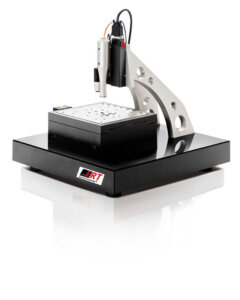
first generation art of metrology

Figure 2: First-generation MicroProf — tabletop version

“From the beginning, we focused on customer needs, offering measurement services primarily for our customers in the automotive and medical markets,” Fries recalls. If they didn’t have the necessary equipment, they rented it from the nearby Max Planck Institute, he said.

In those early years, FRT focused on automotive, medical, optical, and electronics markets. The team saw a need for a high-resolution tool that could measure very small areas and would bridge the gap between meters and nanometers. What Fries envisioned, was a multisensory tool that could be used to measure all surface dimensions. He calls it “bridging the gap from meters to nanometers.” In 1998, FRT’s first-generation multi-sensor tool was built, and the company evolved from being a service organization to an equipment supplier (Figure 2).

Figure 3: Thomas Fries, in the early days of FRT

“We never intended to build and sell tools, we just wanted them to use internally,” says Fries (Figure 3). “But then we realized developing a tool and scaling it was more interesting than doing high knowledge services.”

For the next eight years, FRT found its niche, developing and rolling out the second-generation multi-sensor tool, and continuing to target the automotive and optics, machining engineering and electronics markets, while also maintaining the contract business.

In 2006, as more pioneers of optical metrology entered the optics space, keeping prices low, Fries made the decision to break into the semiconductor market, as this space was being avoided by other players due, in part, to long turn-around times. In Fries’ opinion, the semiconductor industry offered an open playing field (Figure 4).
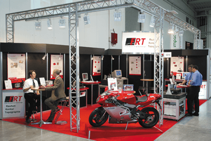
The art of metrology on display

Figure 4: FRT showcasing its services at a trade show in 2006

“This was an opportunity to differentiate our company from the other players, and be unique by focusing on more complex technologies,” explained Fries. “Sure, it was risky, but there’s no fun without risk!”

To get started, FRT developed brand-new multi-sensor tools for the fab. In-house software developers wrote the interface themselves. As they were doing this, the LED industry was ramping up, and with it came a need to measure total thickness variation (TTV) of materials and exotic substrates. This called for a high-speed, high resolution, very accurate optical system, and FRT delivered. It quickly grabbed 100% market coverage of sapphire wafer metrology in Taiwan and 40% in China. It also served the traditional semiconductor and MEMS markets, but the market share was still small.

Figure 5: Metrology tool with material handling unit MicroProf® MHU

The crash of the LED market in 2011 came just as FRT had taken the step from R&D tools to production with fully automated tools in the LED market (Figure 5). As a result, 2012-2014 was a period of struggle for FRT’s sales organization, says Fries. But the company persevered and continued to develop fully automated third-generation metrology tools with a wafer handling system within an Equipment Front End Module (EFEM) for the semiconductor and MEMS markets. By 2015, it had recovered thanks to traction in its original markets: automotive and optical, and big European customers.

FRT: The Art of Metrology

2016 brought the third incarnation of the FRT brand: FRT, The Art of Metrology, along with new assets and a logo change. 80% of its tools were being sold in the semiconductor and MEMS spaces. The company also broke into the advanced packaging market, succeeding with top-tier integrated device manufacturers (IDMs) and memory makers in the USA and Asia.

With the new brand came an enhanced idea about marketing, as well as a change in attitude about metrology. The company focused on its nimbleness and flexibility. When working with customers, Fries and the whole FRT team took a holistic approach, examining each project from the point of view of the customer, and investing in new technology development (Figure 6).

Figure 6: The Wall of Fame at FRT Headquarters

“From 2016-2019, FRT, The Art of Metrology, was one of the companies with the highest annual growth rate,” said Fries. “It became clear that if we were going to continue on this trajectory, we needed a strategy.” Part of this was to create a demo facility and open a new subsidiary, FRT of Taiwan. But expanding a global footprint very fast can be difficult for a small company. Multiple advanced orders can create a cash flow crunch. It was time to consider other options.

FRT: A FormFactor Company

In what can only be described as one of the fastest mergers in recent semiconductor history, in November 2019, FRT, The Art of Metrolgy, was acquired by FormFactor in a simultaneous signing and closing. As part of the deal, FRT will maintain using its well-established brand and operate as a FormFactor company.


Figure 7: I visited with Amy Leong and Mike Slessor at FormFactor’s HQ in Livermore, CA

Ten years ago, FormFactor was primarily a DRAM probe card provider, with a very concentrated and volatile demand profile. In 2012, the company began to diversify by acquiring MicroProbe, the number one supplier of advanced non-memory probe cards, to expand its presence in the foundry and logic markets. In 2016, the company acquired Cascade Microtech, which brought RF probe cards and engineering systems. With the FRT acquisition, the goal was to expand FormFactor’s reach into optical metrology focused on the advanced packaging space, explained Mike Slessor, CEO, FormFactor (Figure 7).

“Advanced packaging is driving our business,” said Slessor, “This is a growth area in the industry, and we are dedicating more resources to roadmap innovation in serving advanced packaging applications.”

Slessor, Fries, and Amy Leong, CMO and VP of M&A for FormFactor all agree that the two companies are a natural fit. FormFactor is a leader in the electrical test for the semiconductor and advanced packaging industry, while FRT’s core competencies are optical metrology and inspection.

“FRT has great technology with good adoption, but to be a world-class supplier, you need the infrastructure and ability to support it globally. As a small company, it’s not easy to grow that organically because it’s expensive to build that infrastructure; but it’s an infrastructure and set of customer relationships that FormFactor already has,” said Slessor.

“We wanted to have a global footprint but lacked the resources to hire and do more development,” Fries explained. “This is the best situation because FormFactor is not active in the optical metrology business. All others (competitors) would have squeezed us out, and that would have been the end of FRT. Now, we are a new business unit. We have the chance to perform. They want to build up the FRT business.”

“We took a broad look at the metrology players, and for a variety of reasons, FRT bubbled up,” explained Leong. “The transition was easy because there was no overlap in technology offerings.” FRT’s focus on metrology and inspection for advanced packaging and niche applications such as silicon photonics was a key selling point, explained Leong. Others included size, scale, and customer engagements, including customer pull for hybrid solutions. (In a happy coincidence, Leong says she first learned about FRT as a company from their presence on 3D InCites.)

The Next Era

January 2020 kicked off a new era for FRT as the company added defect inspection tools for wafer applications to its portfolio. This new capability was customer-driven, said Fries. A customer had a need, and FRT developed the capability.

The modular system is capable of defect inspection down to one micron. It uses image sensing technology to find scratches and particles in wafer samples and then uses metrology to analyze the defect to see if it is a latent or killer defect. It performs full wafer mapping and different types of inspection.

By first looking for rough defects and then only zeroing in on trouble spots with 3D metrology, throughput is increased, explained Fries. The idea is to identify “golden die” and compare it to those with defects.

Customers will be able to order either full inspection systems or combine both metrology and inspection into one tool. Integrating both capabilities into one platform allows for the same software that are components to be used on all tools.

“This offering is unique to FRT. We are the only manufacturer on the market that provides these capabilities in a single platform,” said Fries. “Others have different platforms for inspection and metrology.”

The Art of Metrology Culture

After spending a day at FRT’s headquarters near Cologne, Germany, and meeting members of the team from the executive management to administrative support, it’s easy to see what makes it such a great place to work. The company fosters a diverse and inclusive workplace, with employee representation from 17 different countries of origin. 33% of the workforce are women, the staff is between the ages of 23 and 60 years. The young people bring in new ideas, and the older employees mentor them. In this way, they learn from each other.


In addition to hosting a summer barbeque and Christmas party, there is FRT Day, a team-building event featuring activities and sports. Community outreach includes offering training to primary school teachers along with materials to help teach physics and science to children. Lastly, the company hosts a Technology Night during which they open their doors to the community from 6 pm to midnight so people can come and learn about what they do. This gives students the opportunity to see where they could work someday, explained Sarah Trompetter, FRT’s marketing, and communications manager.

As Dr. Jürgen Koglin, head of applications at FRT notes, the company has always had a family-like atmosphere. “We were a small family at the start. Now we’re a big family,” he says. Koglin joined in 1997, just as FRT was getting started. He knew Fries from his time as his student at the University of Bonn. After receiving his Ph.D. in Physics from the University of Muenster, he joined the company as employee #7. As a result, he was very involved in company decisions. “Everyone was involved in the beginning,” he recalls.

All tool development at FRT is application centered. While they begin with standard tools, the last 5-10% is custom configured. Koglin and his team of five work with customers to perform test measurements and feasibility studies on customer samples to determine what type of sensor, measurement, and instrument is suitable for the customers’ tasks. While the work is technical, the team works closely with the sales team to ensure they recommend the best combination to the customer.

Koglin says that over the years as they work on more intricate technologies, the solutions become more complex. There are many types of applications that must be solved with one tool and different sensor types, but that’s what keeps his job so interesting.

As a department head, Koglin gets to build his own team. He says he looks for motivated people who can think on their own and develop solutions, but also work well on a team, as all projects require collaboration. “It takes about a year to become involved in the techniques,” he said. “So we look for people who will stay at least 3-5 years.”

Bastian Tröger, product management, is another FRT veteran who came to the company straight from academia. Armed with his master’s thesis, in which he constructed a tool for measuring diffraction efficiency, he joined FRT in 2007 as part of the development team and worked his way to product management. He’s been a team leader in PM since 2017.

Tröger reminisced about his days in the cleanroom and how exciting it was as new products were developed. Today his main focus is on typical product management tasks. But he also enjoys working with the field engineers, supporting on-site tool acceptance and application development at customer facilities.

What has kept him there for more than a decade? “If you work here, it’s not a routine job. It’s different every day and there are always new challenges,” he said. “We’ve got a good, collaborative team and we know each other well.”

What’s Next for FRT, The Art of Metrology?

25 years is a good chunk of time in an industry that is barely over 50 years old. In that time, FRT has established a strong foothold in process control for heterogeneous integration technologies. Going forward, as device reliability becomes more and more critical, FormFactor will provide the muscle to take this nimble player to the next level without sacrificing its flexibility, integrity, or company culture. I’m excited to see what the next quarter-century has in store.

The post 25 Years Perfecting the Art of Metrology appeared first on 3D InCites.

Get your copy of LAYERS – Thin-film Technology News in Advanced Packaging

$
0
0

LAYERS 5, from Evatec, is your guide to all the latest thin-film technology news across advanced packaging, semiconductor, 0ptoelectronics, and photonics.

Read about developments at Evatec

Learn about changes in our capabilities and processes that support our customers better for the future.

Advanced Packaging

Read contributions from guest authors SEMCO and GS Swiss PCB and how heterogeneous integration is the answer as we look beyond Moore’s law.

Semiconductor

Guests from ST and ANALOG DEVICES join Evatec’s own authors with stories of innovation across Power Devices, MEMS, and Wireless Communication.

Optoelectronics

Our optoelectronics team reports how we are helping customers solve challenges in the production of Micro LED and OLED on CMOS.

Photonics

From plasma enhanced reactive magnetron sputtering to hybrid optical monitoring find out how Evatec production tools are enabling new levels of process control and new emerging technologies like silicon photonics.

To get your free copy as either pdf or hardcopy simply complete our contact form including your chosen deliver format and address


The post Get your copy of LAYERS – Thin-film Technology News in Advanced Packaging appeared first on 3D InCites.

DAC 2020 Addresses Chiplet Design and Integration

$
0
0

In the early days of ASIC technology, only logic library elements and basic I/Os with up to 10s of transistors were available for customizing gate arrays and/or logic functions in standard cell chips. And then, “megacells” (a.k.a. Functional Blocks, Semiconductor IP Blocks), comprised of 100s, even 1000s, and more transistors became available and offered proven memories, processor cores, data converters, special I/Os and many other widely used functions for integration in IC designs. These megacells enjoyed rapid market acceptance, mainly because they boosted designers’ productivity, reduced risk of failure, and cut development as well as unit cost.

History Repeats Itself

While Moore’s Law has driven major progress in integrating many functions into small pieces of silicon (a.k.a. die, plural dice), IC packaging experts at IDMs, assembly houses (a.k.a. OSATs) and wafer foundries have developed technologies to integrate one or more of these delicate dice into an IC package, primarily to protect it/them against mechanical damage and avoid over-heating. Because advanced packaging technologies have made it technically easier and more cost-effective to combine multiple dice in a package, calls for repeating the success of ASIC megacells for advanced packaging became louder. Developers responded and the term “chiplet” was coined for a die that is ready for integration into a package and can interface with other chiplets in this package.

As a complete product, a chiplet includes not only the physical die but also models/electronic datasheets that describe – e.g. core functionality, physical dimensions, power dissipation, footprint, location of power/test/signal pins and I/O characteristics. These models/electronic datasheets enable EDA planning, design, and verification tools to integrate chiplets relative quickly into a suitable single-die or multi-die package, optimize power, unit cost, reliability, and ensure first-time success. High bandwidth memory (HBM) devices were the first chiplets offered; FPGA slices, SerDes I/Os, processor cores, hardware accelerators, and other functions followed. A chiplets can be proprietary – to differentiate an IC – or available from 3rd parties who specialize in widely used functions – e.g. HBMs and SerDes.

While EDA companies – for business reasons – typically wait for new technology to mature and standards to solidify, before supporting it to automate design steps, the rising market demand for chiplets has encouraged the EDA industry to dedicate time at DAC 2020 for addressing chiplets. Tutorial 10, titled Chiplet Integration: Tools, Methodologies, Requirements, Infrastructure covered in two-parts of many aspects of chiplet design and integration.

DAC 2020 Tutorial 10 – Chiplet Integration

Farhang Yazdani, President & CEO of BroadPak, organized the tutorial, introduced the speakers, outlined the chiplet concept (Figure 1), discussed the role of interposers/substrates, and emphasized the advantages chiplets and advanced packaging offer, compared to single-die SoCs.

Figure 1: Chiplets on interposer/substrate improve performance per Watt, reduce form factor and cost. (Source: BroadPak)

Yazdani also listed many chiplet information sources and addressed a frequently asked question in depth: What interposer/substrate) to use when? Here is a summary:

  • Silicon interposers match the coefficient of thermal expansion (CTE) of chiplets, offer good thermal conductivity, allow L/S pitches of < 1 µm high aspect ratio through-silicon vias (TSVs), multiple redistribution layers (RDLs) and embedding of passives (RLC). However, they are costly (compared to organic and glass), limited in area, and very lossy at high frequencies (e.g. at ~ 60 GHz in 5G mm-wave applications).
  • Organic interposers offer a significantly lower cost per area, can be much larger than silicon interposers, but limit L/S pitches to a few um today. However, they do not match the CTE of silicon – which may lead to cracking of thinned, large chiplets.
  • Glass interposers can match the CTE needed, offer smooth surfaces, can be large, and are ideal for high-frequency designs. However, glass is an insulator – which is good if electrical insulation is needed, but their bad thermal conductivity makes them unsuitable for higher-power applications.

Figure 2: Gordon Moore predicted the need for More than Moore technologies. (Source: Blue Cheetha Analog Design, Inc.)

Krishna Settaluri from Blue Cheetah Analog Design, Inc., outlined how his company’s analog design tools, based on Berkeley’s BAG Framework, automate the generation of analog circuits, specifically designing physical layer I/O circuits (PHYs), compliant with Intel’s advanced interface bus (AIB). He developed the presentation together with David Kehlet from Intel and clearly showed that his team and Intel work together closely, to accelerate AIB market acceptance. To confirm the importance of chiplets, Settaluri showed a previously often overlooked statement from Gordon Moore (Figure 2) that predicted decades ago the need for these IC building blocks.

Sattaluri explained that lack of automation has contributed to making analog circuit design very time consuming and reuse of analog blocks difficult. This challenge has motivated Blue Cheetah Analog Design to develop an analog circuit generator. Together with proven Cadence tools, it increases analog designers’ productivity. To demonstrate this generator’s capabilities, he showed the layout of a 2-channel AIB PHY test chip, taped out for manufacturing in Intel’s 22FFL process.

Ramin Farjadrad, Marvell’s CTO Networking/Automotive PHYs, showed several design examples using silicon interposer, organic substrate, and fan-out wafer-level packaging (FOWLP). He outlined the strengths of each technology and compared their capabilities – e.g. using bit-rate (Gbits/sec), reach (mm) and power consumption (pJ/bit) – of AIB 2.0, HBM2e, HBI, Bunch of Wires (BoW) Base, AQlinkB on silicon interposers, then Kandou Bus, BoW-Fast, AQLinkP and XSR on an organic substrate. Farjadrad recommended BoW, an OCP/OSDA inter-Chiplet interface to use for silicon and organic substrates.

John Park, Product Management Director for Advanced IC Packaging at Cadence, reasoned why system and IC designers demand integration of chiplets in advanced packages and discussed some of the technical challenges for our industry. Figure 3 shows a high-level overview of important design tools/flows/methodologies needed, to optimize die-package-board co-design.

Figure 3: Important design challenges our industry needs to address. (Source: Cadence Design Systems)

Park also explained why data about materials characteristics and accurate electrical, thermal, and thermal-mechanical modeling are essential to optimize performance, cost and reliability of multi-die designs. He showed how Cadence uses its proven as well as newly developed tools to address specific co-design challenges. In Figure 4, Park showed what kind of design tools/flows/methodologies Cadence is developing, to increase system and IC designers’ productivity and enable them to create sign-off quality inputs for manufacturing.

Figure 4: Cadence’s major contributions to sign-off quality multi-die co-designs.(Source: Cadence Design Systems)

Jawad Nasrullah from zGlue emphasized that “Power is Everything” for IC designs, then outlined how zGlue’s ChipBuilder, their Active Silicon Interposer, and the Open Chiplet Initiative simplify multi-die IC design and help to save power. Figure 5 shows a design example with several dice on an active interposer.

Figure 5: Example for a zGlue test case.

Personal Comments

This tutorial was an important step towards addressing chiplet topics – special thanks to BroadPak’s Farhang Yazdani for organizing it. However, based on the most likely DAC audience – EDA developers and IC designers – most presenters focused on design topics and did not or only briefly address manufacturing, test, or material characteristics, all topics important for the 3D InCites readership. That’s why I am motivated again to get on my “soapbox” and ask for better cooperation between EDA & IC Design and manufacturing & test experts. Based on my 40+ years in this industry, I can assure you that all semiconductor supply chain members need to work together more closely, to accelerate market acceptance of innovations and reduce time to profit for all supply-chain members, from EDA developers to IC designers, to IC manufacturing and test experts to vendors of electronic systems.

There is an excellent way to start bridging these gaps. I want to encourage you to read about it on SEMI’s website, then study the work of the pre-competitive technical working groups (TWGs), as they contribute to defining the Heterogeneous Integration Roadmap (HIR). Their efforts are sponsored by a number of major industry associations and address both important market requirements as well as development challenges. The TWGs focus on die-package-board co-design as well as manufacturing and test requirements of major applications. They talk to each other extensively, to synchronize development efforts with future market requirements. (FYI: HIR has replaced the die focused ITRS Roadmap because today’s and future challenges cannot be met with single die SoC solutions alone.) Figure 6 provides an overview of the currently active TWGs. The pointers in the following paragraph lead to much more information about HIR accomplishments, activities, and plans.

Figure 6: Heterogeneous Integration Roadmap (HIR) overview. (Source: HIR and eda 2 asic Consulting, Inc.)

Please check/download/study for free:

  • The 2019 edition of the Heterogeneous Integration Roadmap here
  • he recordings of many Technical Working Group presentations here
  • Please email Denise Manning at IEEE/IPS if you want to join/contribute to a TWG  ~Herb

The post DAC 2020 Addresses Chiplet Design and Integration appeared first on 3D InCites.

Technologies Migrate from Both Directions to AP Processes

$
0
0

Advanced packaging (AP) processes are often described as the front-end-like processes that have migrated to traditionally back-end applications for packaging semiconductor devices. However, AP processes also draw on techniques developed in the other direction, downstream from packaging at the assembly level, where packaged devices are connected to each other on printed circuit boards (PCB), typically using surface mount technologies (SMT). Just as features are scaled up from their front-end sizes to connect devices in AP processes, they are scaled down from the SMT/PCB world, ultimately comprising a size range from about 10µm to 100µm that has been called the “middle-end”.

Many of the techniques used in SMT, especially inspection and measurement, can be scaled successfully for AP applications. The evolution of high-resolution, phase shift profilometry (PSP) is one example. The technique’s ability to provide fast, accurate, 3-dimensional characterization has earned it a central role in SMT processes. Now, the latest generation of sensors (Nano Resolution MRS™, CyberOptics Corporation )provides nanoscale sensitivity to height variation and micrometer-scale spatial resolution at production-worthy speeds that are significantly faster than alternative technologies.

In adapting PSP technology to AP sensors, engineers were challenged to increase the resolution of the optical system while preserving the technique’s high speed. Another, less obvious, hurdle was the need to measure specularly reflective surfaces, such as solder bumps, for which accurate 3D measurements of height and coplanarity are critical. Conventional PSP technology requires a diffuse reflection from the measured surface. The new sensor includes a dedicated channel for specular surfaces that provides fast, accurate measurements.

Phase Shift Profilometry

PSP uses structured light to measure the topography of a surface (figure 1). It projects a pattern of light and dark fringes onto the surface from one direction and views the surface from a different direction, looking for distortions in the pattern caused by changes in surface height. If the pattern is a series of straight, regularly spaced fringes projected from directly above the surface, and the surface is perfectly flat when viewed from a different angle the fringes will remain straight and parallel. If there are bumps or depressions in the surface, the fringes will appear to curve or shift. Knowing the difference between the projection and observation angles and measuring the direction and magnitude of the shift, we can calculate the change in surface height. Since the intensity of the fringe varies sinusoidally, we can measure exceedingly small shifts in its position. The “shift” in phase shift technique derives from shifting the sinusoidal pattern by known increments (e.g.. 90 degrees) to solve for reflectance, fringe contrast, and the phase.

Figure 1: Phase shift profilometry converts shifts a projected fringe pattern into measurements of surface height.

The calculation becomes slightly more complicated when the surface has abrupt changes in height, such as a feature with a flat surface and vertical walls. The fringes will show discontinuous shifts where they cross such a feature. The size of the shift still indicates the difference in height, but the direction and magnitude of the shift are no longer obvious. Did the surface change up or down? Did the fringe shift half a fringe or one and a half fringes? There are ways to eliminate these ambiguities and other measurement limitations by using multiple patterns with different frequencies and orientations, and multiple cameras to view from different perspectives.

One of the great advantages of PSP is that it is an image-based technique that captures data from the full field of view simultaneously, makes it much faster than alternate technologies. Using multiple cameras viewing from different directions multiplies this advantage by capturing multiple images simultaneously. The translation of measured phase shifts into height variations, known as unwrapping, is performed by sophisticated software routines that run with extraordinary speed on modern graphic processors. In practical terms, our latest sensors can inspect the full surface of as many as twenty-five 300mm wafers per hour with 50-nanometer height resolution and 3µm spatial resolution.

Specular Reflections for AP Processes

Specular (mirror-like) reflections are an example of one of the hurdles facing engineers in adapting PSP to advanced packaging applications. Specular surfaces on features like solder bumps and pillars are common and their measurement is critical to ensure the integrity and reliability of vertical connections between stacked chips or between chips and substrates.

Figures 2a and b illustrate the twofold challenge of specular surfaces for conventional PSP: 1) spurious multiple reflections between specular surfaces can introduce errors in the measurements and 2) the projected fringe pattern is not visible on a specular surface.

specular reflections for AP processes

Figure 2: Specular reflections pose significant challenges to phase shift profilometry measurements. (Left) Multiple specular reflections among shiny features, such as solder joints, tinned leads, and metal oscillators, can cause distortions in the fringe pattern and errors in the height measurements. (Right) The projected fringe pattern is invisible on specular surfaces. The two, round features are identical, except that the upper one has a diffusely reflective surface and is mounted on a similarly finished flat surface, while the lower one has a specularly reflective surface and is mounted on a flat mirror. The projected vertical fringe pattern, clearly visible on the diffuse surfaces, disappears on the specular surfaces.

Spurious multiple reflections occur when bright light falling on one feature is specularly reflected with another feature and then back to the sensor, giving an erroneous reading of the fringe intensity for that point. Because specular reflections are highly directional, comparing images from multiple cameras provides one way to detect and eliminate their effects – they are unlikely to appear the same from different directions. Likewise, they are unlikely to appear the same when illuminated by fringe patterns with different spatial frequencies (figures 3a and b). The combination of these and other analytical techniques allows us to successfully reject spurious reflections in our MRS (multiple reflection suppression) sensors.

Figure 3: Multiple reflection errors can be suppressed by analysis from multiple directions at multiple frequencies. Reflections that add coherently at lower frequencies become incoherent at higher frequencies, reducing fringe contrast but not affecting the phase measurement.

The second challenge, measuring specular surfaces, requires a different approach. Conventional PSP relies on measuring the intensity of a diffuse (non-directional) reflection from the measured surface that is representative of the intensity of the projected pattern at that point. Although we cannot see a shadow on a mirror, we can tell something about the shape of the mirror surface by analyzing its effects on the reflected image (Figure 4). In this analysis, the mirror surface is treated as an element in the optical path. Our latest generation of MRS sensors includes an additional channel dedicated to measuring specular surfaces with optical analysis of the reflected light.

Figure 4: Magnified views of the diffuse (left) and specular (right) features shown in figure 1 above. The vertical fringe pattern is projected from a direction roughly perpendicular to the mounting surface. The rectangular grid pattern is printed on a flat surface that is also perpendicular to the mounting surface. The projected vertical fringes clearly reveal the shape of the diffusely reflective surfaces when viewed from a direction somewhere between the projection axis and the surface, but the fringe pattern is invisible on the specular surfaces. Rather, we see the reflected image of the printed grid pattern. By analyzing the reflected image, treating the specular surfaces as elements in the optical path, we can characterize the shape, position, and dimensions of specular features and surfaces.

To remain profitable, electronics manufacturers must continually monitor process performance to detect and correct problems and ensure yield. Inspection and metrology are the indispensable foundation of process control. In the same way that process technologies are converging in advanced packaging processes, inspection and measurement technologies are migrating from both directions, front- end and back-end, to the new middle-end. With its high speed, nanoscale resolution, ability to measure reflective surfaces, and proven track record in SMT applications, MRS technology is poised to assume a central role in AP process control.

The post Technologies Migrate from Both Directions to AP Processes appeared first on 3D InCites.

IFTLE 458: The Demise of US Chip-making Accelerates as Intel Falls Further Behind

$
0
0

Back in the late summer of 2018 IFTLE unleashed one of its more sarcastic cartoons to note that GlobalFoundries had just announced it would no longer try to compete at the latest node. (See IFTLE 395 “And Then There Were 3…”)

Is Intel Next?

Intel drops out of the game

Well, the remaining three mega players continued their game of Texas Hold ‘Em into the night, and now the last US-based player in the logic game, i.e. Intel, has made an announcement of its own. At Intel’s earning call the end of the 2nd quarter CEO Bob Swan stated that “The company’s 7nm-based CPU product timing is shifting approximately six months relative to prior expectations. The primary driver is the yield of Intel’s 7nm process, which based on recent data, is now trending approximately twelve months behind the company’s internal target……We now expect to see initial production shipments of our first Intel-based 7nm product, a client CPU in late 2022 or early 2023“. By comparison, TSMC plans to be on the 3nm node in the same time frame as Intel’s new schedule for 7nm (a 2-node difference).

According to Swan Intel has identified a “defect mode” in its 7nm process that caused “yield issues”. He added that the company would be using external foundries for its forthcoming 7nm Ponte Vecchio GPU graphics chips. So, Ponte Vecchio, a chiplet-based design, apparently will have some of its chiplets outsourced. Intel’s announced 7nm server CPUs (Granite Rapids) will now be scheduled to arrive in 2023. Swan further stated that Intel could use third-party foundries for entire chip designs in the future. Intel has used outside fabs, for low-margin, non-CPU products built on trailing-edge nodes. But never for its state of the art (SOTA) products.

The announced 7nm delay is added on to the back of a company (Intel) that is still struggling to overcome the embarrassment of its multi-year delay issues at 10nm. The industry is still awaiting Intel’s first 10nm desktop CPUs, which are now not scheduled to arrive in late 2021.

Intel has allowed competitors, like AMD, to take the process node leadership position for the first time in the company’s history.  Apple has also recently announced that it is transitioning from Intel’s chips to its own ARM-based 7nm silicon. Did Apple have advanced notice that Intel would make this announcement?

Some are questioning whether this 7nm delay is simply the beginning of another series of delays like we saw for 10nm. Further, will the 7NM slippage push Intel into a “fab lite” mode? That would make both Intel and AMD dependent upon TSMC. Will Intel really turn its leading-edge manufacturing over to TSMC? At the proposed TSMC AZ fab perhaps?

I may be wrong, but I don’t think there is enough proposed capacity being planned there to supply US company needs.

How does this announcement affect the recent Chips for America Act? [see IFTLE 455 “Advanced Microelectronic Coming Home”]

It has also become clearer that Intel’s capability of using advanced packaging to mix and match die/chiplets in a system-in-package (SiP) has become even more important. But even there, Intel was in catch-up mode. Let’s watch out for those who will try to change historical facts. Bryan Black and AMD drove chiplet technology, not Intel.

If Intel does lean more on its packaging technology to try to maintain equivalence to those using more advanced nodes, the competition, will such production be done by Intel in the US?

And on the Memory Front…

So, while the US now appears significantly behind on SOTA logic nodes, what about memory? There are only three major players left at the poker table in memory – Samsung, SK Hynix, and Micron. In 2011 Micron placed a major bet on the “Hybrid Memory Cube” or HMC as it was to be called. They created a large consortium (which included Intel) to develop this memory technology which featured a low-width bus and extremely high data rates to offer memory bandwidth that exceeded that of then standard DDR3. While HMC did see some minor usage in the market it ultimately, it lost the battle against high bandwidth memory (HBM/HBM2), which were supported by SK Hynix and Samsung, and Micron finally folded the project in 2018. This has put them several years behind the memory eight ball since that time. In April of 2020 IFTLE  reviewed the status of memory technology in IFTLE 447 “Micron and Rambus Readying HBM2 3D Stacked Memory Products”

At the end of Q1 2020 Sanjay Mehrotra, president and CEO of Micron stated: “In Q2, we began sampling 1Z-based DDR5 modules and are on track to introduce high-bandwidth memory in calendar 2020 ” We are currently only in the 3rd quarter so…..we’ll see.

So, playing catch up in both logic and memory, it will be interesting to see how this plays out against the US announcing its desire to bring SOTA chip production back onshore. We better have a well thought out plan and the right people in place to ensure said plan is carried out. This might very well be our last chance to bring the leading edge of this ultra-important industry back home.

Does anyone out there really think money and/or tax breaks is what Intel requires to regain the technology lead over TSMC?? Think this through and don’t screw this up, Washington bureaucrats.

For all the latest on Advanced packaging stay linked to IFTLE………………….

The post IFTLE 458: The Demise of US Chip-making Accelerates as Intel Falls Further Behind appeared first on 3D InCites.


SEMICON West 2020: Sentiment, Sustainability, Diversity and Pandemic

$
0
0

Another SEMICON West has come and gone. Well almost gone, this one will be with us virtually until mid-September.

SEMI’s 50th SEMICON West wasn’t the celebration that they expected; however, I think it turned out all right, considering the circumstances. As Larry Broome posted “my feet hurt less, the food was better and cheaper, and the bathrooms were cleaner”; although, I personally missed the crab cakes and the sushi typically served at the TEL networking party.

As a virtual event, I was able to attend or listen to all of the talks; typically, I need to pick and choose which ones I will listen to when I attend live. Because I have a day job, I appreciated being able to listen to the talks over the period of multiple days, and go back and re-listen to what I didn’t quite catch the first time. However, I was extremely disappointed that former Vice President Al Gore’s talk was not available on demand. This was extremely frustrating for executives and people like me who thought they would be able to review this at a later time, especially since SEMI had indicated it would be available online for some period of time. The good news is that most of the material is available here until September 20, 2020, so you can relive the 2020 Semicon for some time to come.

Watching SEMICON West Grow Up

Because I attended my first SEMICON West in 1983 at San Mateo, I missed out on the first several, but have attended every SEMICON West since. I have a long history with the show and SEMI. I am probably one of the few that attended as a buyer, seller, and then pundit, and now more along the lines of a reporter.  In the early days, there was working equipment at the show; or at least you hoped it would work. In addition to your sales and marketing teams, you had a team of technicians whose job it was to make sure the equipment performed while at the show. The show was about new equipment releases, forecasts, and meetings in the motorhomes. Purchase orders would be submitted on the show floor if customers were impressed enough with the new equipment.

Until SEMI started charging admission, there were a considerable number of engineers, operators, and technicians that would attend the show. While most of these were not decision-makers, they were all users, and some of the feedback you would receive was insightful; about how your equipment was perceived in the fab, and you also might gain some competitive information.

The majority of the companies set up in the exhibition halls at the fairgrounds. As the show expanded the new arrivals were located in the grandstands, so you would occasionally see (and definitely smell) the horses as you made the trip. I always wondered if the fact that Novellus was in the grandstands away from the rest of the show had anything to do with the decision for Rick Hill to use the Yerba Buena area when the show moved to San Francisco.

The move to Moscone was both a location and a date change, from before Memorial Day weekend to after the Fourth of July weekend. So instead of having a long weekend to relax after the show, we now had a long weekend to prepare for the show and then collapse afterward. Initially, with the move to San Francisco, there was also a show in San Jose for the metrology and back end equipment. This caused a bit of gnashing of teeth as some companies had booths in both places, and as an analyst, you would need to spend time at both events. The completion of Moscone West made it possible for everyone to be in the same location.

As was mentioned in the reminiscing webinar, the larger equipment companies slowly moved off the show floor into hotels. As this happened, smaller components companies moved in to take their place. The transition continued as the show became a place to communicate more with Wall Street, and so investor meetings became a significant part of the show.

Sustainability, Diversity, and the Digital Divide: Opportunity and Missed Boats

For the past 2 years, the keynote has seemed to focus on how AI will drive the semiconductor industry forward. This year’s talks touched on the importance of AI, but more on how AI may help to solve the pandemic, or perhaps better predict the next one, so we could be better prepared. SEMI and Applied Materials (AMAT) managed to create a strong focus on sustainability and conservation.

Many speakers discussed the detriments of carbon build-up and have committed to a carbon-neutral business in the future. Art de Gues gave some practical advice on how to personally reduce your carbon footprint.

Renewables

Francoise covered and commented on the major energy speakers in her blog so I will not revisit that here, but I think this is one area that SEMI missed the boat regarding progress in renewables. In recent years solar was part of SEMICON West. This year, not so much, although in the past year there have been some fabulous news on the green energy front. Renewable energy consumption surpassed coal. That is fantastic news that should have been highlighted by at least one of the speakers at the show.

SEMICON

Source: U.S. Energy Information Administration, Monthly Energy Review


Even more important is that the storage of renewables has taken a huge leap in the past few years and instead of just solar or wind farms being built, they are being combined with storage facilities. This means when the sun goes down or the wind stops, renewable energy can still be supplied, and you don’t have to fire up a carbon burning facility to keep the energy flowing to the grid.

Diversity and Inclusion at SEMICON West

Diversity, inclusion, and the new workforce had more focus than I remember in the past. SEMI has had the smart workforce pavilion for a number of years to help attract new talent. However, in an extremely cyclical industry that would hire when things were going crazy and then layoff when the industry turned slower, it can be difficult to attract talent, when you might get laid off the next year.

One talk that really resonated with me was the discussion with Gayle Jennings-O’Byrne. In my time as a hiring manager it was rare to find a person of color that was interviewing for a position as an engineer, or as an analyst. So, it was refreshing to hear that there is a very active diverse tech community, that according to Jennings actually perform better than their counterparts. I’m hopeful that some of the equipment and semi companies’ VC’s were listening and that they will steer some money to Gayle’s fund to support this diversity in the tech industry.

To my simple mind, improving diversity is about creating opportunities for people to succeed. I was fortunate enough to have joined a company that gave me extensive training that was a significant help in my transition from academia to the industry, if that exists today, I’m not aware of it. There are intern programs that cover part of this, SEMI works hard to introduce high school students to the tech industry and just announced a partnership with GLOBALFOUNDRIES to create an apprentice program, but I think more is needed, and it is up to companies to implement the training and create the opportunity for new blood in the tech space.

The Digital Divide

Another missed boat: Closing the gap on the digital divide. This is a huge opportunity for the tech industry to step up and give back. I live in a community where there is a significant digital divide. There is only one internet provider that has the bandwidth for video conferencing, and if you are making minimum wage it is cost-prohibitive to use that service. When distance learning started, the district noticed that students were falling behind or did not have the wherewithal to distance learning. The district provided laptops, hotspots for those families that could not afford the internet, and the teachers followed up with their students to ensure they were keeping up. There are many school districts in the United States that do not have these resources. The Wall Street Journal has done a good job of covering this in a recent article by Tawnell Hobbs titled, “Are They Setting Up my Children for Failure? Remote Learning Widens the Education Gap?”

The author describes a community in Mississippi that does not have the technology resources, and how parents tried to cope to keep their children from falling behind. What an opportunity for tech companies to step in and help level the playing field, create opportunity, and to introduce and educate students about a career in technology! Helping to provide equipment, making sure the internet is accessible for all, and creating the educational opportunity for success would go a long way in making a more diverse workforce. Possibly something for SEMI to think about having speakers discuss in next year’s show.  ~ Dean

The post SEMICON West 2020: Sentiment, Sustainability, Diversity and Pandemic appeared first on 3D InCites.

ISES 2020 Highlights Asia’s Advanced IC Packaging and HI Capabilities

$
0
0

Several decades ago, Asia began its quest to be a reliable and cost-effective IC packaging, assembly, and test partner for low complexity ICs. Since then, Asia has proven itself as the world’s dominant wafer manufacturer and developer of process technologies, down to smallest feature sizes.

On August 4, 2020, I had the opportunity to join, together with about 150 US-based semiconductor experts, an International Semiconductor Executive Summit (ISES) webinar that demonstrated Asia’s current capabilities in advanced IC packaging and heterogeneous integration (HI), as outlined by executives from Samsung and Amkor.

Salah Nasri, Executive Managing Partner ISES, introduced ISES Global, the webinar’s agenda, presenters, and moderator: Dae-Woo Kim, Corporate VP, Head of Advanced Packaging Development Team at Samsung, and Mike Kelly, VP Advanced Package and Technology Integration at Amkor Technology were the presenters. Amy Leong, Chief Marketing Officer and Senior VP, Mergers & Acquisitions at FormFactor, moderated this webinar.

Samsung’s Advanced IC Packaging Capabilities

Dae-Woo Kim emphasized that as feature-size shrinking is getting more difficult and very costly, “More than Moore” (a.k.a. advanced IC packaging, multi-die packaging) is, in most cases, a better way of packing more functionality into an IC package and with it, continues growing opportunities for our industry. Kim sees the need for much higher bandwidth than single-die ICs on a printed circuit board can offer as a key reason for multi-die packaging. He showed examples for integrating multiple chiplets (a.k.a. bare dice) in a 2.5D IC and listed chiplets’ technical and business benefits, also applicable in wafer or panel-level packaging.

Kim explained Samsung’s hybrid bonding technology and its integrated stack capacitor (ISC), that reduces mid/high-frequency noise. Last, but not least, Kim addressed my favorite subject: die-package-board co-design. With the increasing complexity of multi-die IC packaging solutions, challenges like IR drop, supply noise, crosstalk, signal degradation, thermal-mechanical interactions, and other factors in a die-package-board assembly, need to be analyzed in context.

Amkor’s Advanced IC Packaging Capabilities

Mike Kelly presented a very visionary message and outlined the different requirements and trends in the mobility market, in the Internet of things (IoT)/consumer applications, automotive, and high-performance computing (HPC) and networking systems. For example, mobility devices demand 5G and a tiny form factor. IoT edge nodes need high levels of heterogeneous integration and ultra-low power designs. And for automotive, reliability is the dominant criterion. Data Centers need performance, very high levels of integration, and excellent heat management. These significantly different requirements, and frequent needs for customization of packaging solutions, confirm the importance of having clear hand-off criteria between customer and assembly partner and demand an excellent working relationship for successful cooperation.

Kelly addressed another significant trend: The rapidly growing need for even more wireless communication links. In Figure 1 he explained the importance and growth of radiofrequency (RF) applications, showed the major RF building blocks – dominated by RF front-end modules (RFFEMs) and discrete components – as well as the variety of radios needed. Kelly emphasized that new materials with low dielectric loss angle/tangent (a.k.a. low insertion loss) are needed, to avoid/minimize self-heating and signal loss at 5G frequencies in the tens of GHz (FR 2 band / mm waves).

advanced IC packaging

Figure 1: RF building blocks and growth forecast by YOLE Developpement (Courtesy: Amkor Technology, Inc)

Besides RF challenges, Kelly talked about other major packaging requirements  – like form factor reduction, high-power management, electrical-thermal-mechanical interactions – that challenge IC assembly houses and their suppliers. He said the future of packaging will mean solving those challenges by meeting innovation milestones including:

  • Complex modular systems for miniaturization
  • Electrical microsystems targeted to IoT, 5G and AI
  • Electrically and mechanically advanced materials
  • Power dissipation to andle higher power density

It is well known that artificial intelligence (AI) and machine learning (ML) are now deployed widely in data centers. Kelly stated that AI/ML functions are also needed in IoT edge nodes, to minimize local control systems’ response times, reduce network data traffic and power dissipation.

Big data capture, transfer, storage, and compute are today’s major challenges for the semiconductor industry in general, and specifically for IC packaging experts. Figure 2 shows a typical data flow from the edge node to the data center.

advanced IC packaging

Figure 2: Data flow and cross-sections of highly integrated advanced IC packages. (Courtesy: Amkor Technology, Inc)

Another significant packaging trend: Customers want chiplets (a.k.a. bare dice, semiconductor IP building blocks in die-form), to reach far beyond the complexity limits of single-die SoCs, cut time to market, keep design risk manageable, and, most importantly, lower development and unit cost. Chiplets enable the integration of heterogeneous functions (logic, memories, analog, MEMS, etc.), each function manufactured in the most suitable and cost-effective process technology. Fig 3 shows a few of the benefits chiplets offer and how they enable them to integrate (sub)systems into an IC package.

Figure 3: Benefits of using chiplets for system re-integration. (Courtesy: Amkor Technology, Inc.)

To utilize the full value chiplets can offer, the connections between them, to the package and the board, need to minimize bit error rates, signal delays, and power dissipation (measured in pico-Joules per bit) as well as maximize bandwidth.  Kelly showed how packaging experts have reduced bump heights/diameters from 70 / 70 µm to 10 / 15 µm and further to single digits, to meet these requirements. Amkor is also developing hybrid bonding techniques that will allow sub-micron pads and pitches in the future.

As emphasized above, IC packaging experts have to serve many different applications. To do so, Amkor has developed a broad range of packaging technologies – e.g. FC-MCM, 2.5D & TSV, HD Fan-out (SWIFT), and bridge & HDFO (S-Connect).

Personal Comments

Giving management-level overviews of Samsung’s and Amkor’s advanced packaging capabilities in less than 30 minutes each was clearly challenging. It obviously did not allow us to address other important topics, like progress in wafer-probe and test, package assembly design kit (P-ADK) development, nor materials characterization and modeling techniques.

Still, these brief presentations conveyed very clearly that a significant part of a system’s value creation is moving to advanced IC packaging. It enables heterogeneous integration, much smaller form-factors than single-die SoCs, mounted on PCBs can ever reach. Above all, smaller dimensions mean higher system performance, while reducing system power consumption and total system cost.

The post ISES 2020 Highlights Asia’s Advanced IC Packaging and HI Capabilities appeared first on 3D InCites.

How is COVID 19 Impacting the Semiconductor Industry’s Diversity and Inclusion Efforts?

$
0
0

A headline on CNN Business caught my eye last night: Working mothers are quitting to take care of their kids, and the US job market may never be the same. I started reading and went down a rabbit hole of related articles that revealed a few things: Unlike the recession of 2008, this “pandemic recession” is impacting more women than men, and according to the IMF, may “roll back gains in women’s economic opportunities.” This is not only because more women are being laid off due to the sectors hit hardest such as hospitality and tourism, but also because women shoulder more of the childcare burden and are choosing to sacrifice careers for their families.

By pure coincidence, this topic of discussion also came up during our monthly SemiSister Happy Hour, as those of us with children of all ages at home, from infancy to college, shared how they were juggling their jobs and the needs of their families while working from home. Bottom line: it’s not easy to focus with a toddler clamoring for attention, or a teenager who’s trying to get out of doing online schoolwork.

In a separate but related conversation with my daughter, who just started a Ph.D. program in pharmaceutical sciences, l learned that she was one of only two candidates in her program because of international visa restrictions due to COVID 19. Several of her colleagues from China were still trying to get their visas.

All this got me thinking about all the work our industry is doing to create diversity and inclusion in the workplace. What impact will COVID have on these efforts? Let’s take a look.

Diversity and Inclusion is Good for Business

Both ECTC and SEMICON West featured diversity and inclusion panel discussions and presentations about how to recruit and retain a diverse and inclusive workforce. In her recent blog summarizing presentations at SEMICON West, Margaret Kindling cited the growing body of research that shows how diversity and inclusion is just plain good for business: it fosters innovation and productivity and improves profitability. Diverse teams solve problems faster and make better decisions. This extends beyond merely gender diversity to include different ethnicities, races, socio-economic backgrounds, and the LGBTQ+ community.

Why Is It so Hard to Find and Retain a Diverse Workforce?

Despite the clear understanding of the benefits of diversity and inclusion in the workplace, data show that the needle is moving slowly, and in some cases, it’s moved in the wrong direction.

In her ECTC presentation, Allyson Hartzell, Veryst Engineering, provided some sobering statistics showing that between 1982 and 2017, the female engineer population in the United States rose a mere 8.1%. “I’ve been working for 38 years and I thought it would be better than this. I thought it would be 50% by now,” she said. “The data is miserable. We have to do better because we can’t do worse. This is a national tragedy.”

The problem begins at the university level, where, according to this article by Mark Crawford, of ASME, women are still battling stereotypes, lack female engineering role models, and have misconceptions of what it is like to be an engineer. Despite performing better than men, they are more likely to change their major because they lack confidence in their own skills.

Additionally, once women have engineering degrees, data shows that they are more likely to work part-time than men because between professional careers, parental responsibilities, and general caregiving, women continue to have more roles (Figure 1).

Figure 1: Employment status by gender. (Courtesy of Alyson Hartzell)

Hartzell also looked at statistics for underrepresented minorities (Black, indigenous, people of color (BIPOC), Hispanic, and Latinx) —including men, women, and LGBTQ+, and noted a decline in master’s degrees due to lack of available funding in the past few years. (Figure 2)

diversity and inclusion statistics

Figure 2: Under-represented minorities in science and engineering degrees. (Courtesy of Alyson Hartzell)

She drilled down further to peel away the layers of STEM type degrees for BIPOC women only, and while bachelor’s degrees in psychology are on the rise, over time, degrees in engineering, computer science, and math are declining among this cohort (Figure 3).

diversity and inclusion statistics

Figure 3: BIPOC B.S. degrees by field. (Courtesy of Alyson Hartzell)

What Can We Do About It?

Lots can be done, but we can’t expect change to happen overnight. It begins by changing the stereotypes communicated to girls and boys as early as middle school and continues through university. On the hiring front, it requires changes to recruitment practices and continues with building a culture of inclusion. As Lam Research’s Lubab Sheet-Davis says, “Diversity is a metric. Inclusion is a practice.”

Recommended recruitment practices include:

  • Using inclusive language in job postings
  • Casting a wider recruitment net by using social media platforms, career fairs, career sites, and educational institutions that serve minorities
  • Consider alternatives to high-level degrees as job criteria, such as training programs and apprenticeships
  • Assemble a diverse hiring committee trained in diversity and inclusion
  • Set a consistent set of evaluation procedures and stick to them
  • Call out inclusive benefits such as maternity/paternity leave and flexible hours

I don’t have to look much farther than to members of the 3D InCites community to see that this message has taken a firm hold at many companies in our industry. They have implemented initiatives to not only improve the numbers but to create an inclusive culture so that employees want to stay.

In a video interview with FormFactor’s senior manager of talent acquisition, Sarah Shield, she talked about the company’s STEMinist initiative. She defines the word as “A champion for equal representation in science, technology, engineering and mathematics field.” You can watch the video here.

At Brewer Science, as of 2019, 40% of its executive team are women. Overall, the company Averages 10-25% more women in technical jobs, leadership roles, and total workforce than most technology leaders in the semiconductor industry. Brewer Science does a considerable amount of community outreach to promote STEM education, such as a summer internship program for teachers who then take back the skills they learned to their classrooms.

At FRT, employee representation comes from 17 different countries of origin, 33 percent of which are women between 23 and 60 years. The company’s hiring strategy is completely independent of gender or sexual orientation. Unique characters are underlined with positive appreciation, and individuality is encouraged.

Finally, at SPTS as of 2019, 22% of recent graduates hired and 15% of the apprentices are women. The company is focusing on increasing the number of female recruits through more female representation in recruitment material and events. The company is also involved in a Women in STEM initiative with the Welsh Government and participate in a STEM Ambassador program. Enhanced benefits to increase retention, including maternity and paternity leave and flexible work hours for all, has resulted in 100% of employees returning after maternity leave.

So back to the original question: What impact will the pandemic have on D&I efforts? Unlike other industries, it may turn out to have a positive effect, as working remotely proves to be as productive as working on-site and allows for hiring from anywhere in the world for any job. Only time will tell.


The post How is COVID 19 Impacting the Semiconductor Industry’s Diversity and Inclusion Efforts? appeared first on 3D InCites.

Scientech Corporation and Trymax Partner to Distribute Resist Ashing and UV Products in Taiwan

$
0
0

NIJMEGEN, The Netherlands and SANTA CLARA, California (Aug. 24, 2020) — Trymax Semiconductor Equipment BV, a global leader in semiconductor plasma technology, and Scientech Corporation, announced today that they have entered into a distribution agreement for Taiwan. The agreement gives Scientech Corporation the right to distribute all of Trymax’s NEO ashing, etching products and the latest UV curing and charge erase products.

This agreement with Trymax will assist Scientech in expanding its business in the segment of high speed communication, 3D sensing including ToF, high frequency power devices and related device markets. Scientech offers extensive experience in introducing the highest quality equipment from around the world and will provide world-class technical and field support for Trymax products after system delivery.

“A partnership with Scientech is a critical component for our expansion strategy in Taiwan” stated Ludo Vandenberk, Executive Vice President of Trymax Semiconductor Equipment. “By combining forces with Scientech, we are able to better serve the front-end, MEMS and back-end manufacturers with solutions that span the ashing, descum and lite etch process steps as well as the UV curing and charge erase applications. We are eager to get started serving our customers with the competitive advantages that our technologies can offer.’’

“With Trymax’s expertise and cost-effective solution, we are very grateful to cooperate with Trymax to support the customers in the semiconductor field, which is not only to enhance our coverage of front-end production but also strengthen our customers’ competition in the arena.” commented Peter Kuo, Vice President Representative Div. II at Scientech Corporation.

Trymax’s NEO products for ashing, etching and descum serve the semiconductor industry for 150mm, 200mm and 300mm substrates. Our bridge tools are fully flexible for processing multiple different substrates types like Si, GaAs, SiC, LiN, LiT, eWLB™ and Taiko™ wafers from R&D to high volume production. We offer optimized solutions based on the best cost of ownership in combination with the maximum flexibility. All Trymax platforms are having a fully digital onboard communication system with up to 5 different process chamber technologies selectable.

UV curing and charge erase equipment from Trymax are used for a wide range of applications that includes photo-stabilization of the resist prior implantation or etch, for small CD, or to erase charge built-up during the IC manufacturing process. The NEO 2000UV has been designed taking advantage of the reliable NEO platforms developed by Trymax for plasma ashing, descum, and etching applications. The NEO 2000UV is implementing state-of-the-art robotics, components, the latest digital technologies and software, and is CE compliant. NEO 2000UV can accommodate cassettes or SMIFs.

About Scientech Corporation:
Scientech Corporation (www.scientech.com.tw) was established in 1979 and has headquarters in Taipei, Taiwan, with five additional offices across Taiwan and 10 offices in China. Scientech will provide full sales, installation, service, parts, process development assistance and technical support for all representing equipment, tools and products.

About Trymax Semiconductor Equipment BV:
Trymax’s core business is to support semiconductor manufacturers through the world with innovative plasma-based solutions for photo resist removal, surface cleaning, isotropic etch, as well as UV curing/charge erase, that are used in the fabrication of integrated circuits and other semiconductor devices. Trymax is a privately held company headquartered in Nijmegen, The Netherlands. Trymax operates regional offices in China (Suzhou) and Italy (Milan). Learn more at www.trymax-semiconductor.com.

Company contact:
Ludo Vandenberk
Executive Vice President
+31 24 350 0809
Ludo.vandenberk@trymax-semiconductor.com

The post Scientech Corporation and Trymax Partner to Distribute Resist Ashing and UV Products in Taiwan appeared first on 3D InCites.

IFTLE 459: imec Develops Nano-TSV for Heterogeneous Integration

$
0
0

This week we continue our look at ECTC 2020.

imec and SPTS Collaborate on Nano-TSV Processes

As part of our IFTLE theme of advanced packaging and interconnect going submicron, let’s look at the imec (long renowned for both their front end and back end work) presentation “Extreme Wafer Thinning and Nano-TSV Processing for 3D Heterogeneous Integration” by Anne Jourdain (Figure 1)

Nano-TSV

Figure 1: The 3D interconnect technology landscape. (Courtesy, imec)

To reach sub 500nm interconnect pitches, they had to develop an extreme wafer thinning process with total thickness variation (TTV) thickness control over the full wafer and nano through-silicon via (nano-TSV) with a modified Bosch etching process. Using these processes, they have achieved 99% electrical yields between the front and backside of the devices.

The impact of the wafer-to-wafer bonding process on the TSV photolithography with respect to metal 1 must also be characterized.

IMEC is looking into 0.7µm TSVs with 5µm depth. By further thinning the silicon from 500 to 300nm, the TSVs become nano TSVs with diameters of a few 100 nm.  Such thinning requires etch-stop layers and several thinning processes in order to obtain the required dimensional control. The TSV process and the extreme wafer thinning process are shown below (Figure 2 and Figure 3).

Nano-TSV process

Figure 2: Front-end processing with metal tracks. (Courtesy of imec)

Nano-TSV process

Figure 3: Extreme wafer thinning. (Courtesy of imec)

This requires grinding, dry etch, and wet-etch processes.

After wafer thinning to ~500nm they deposit a thin oxide layer (150nm of low-temperature oxide) as backside passivation. The nano-TSVs are aligned to the backside side metal. 150 x 110nm TSVs are filled with copper.

Nano- TSV alignment is a complex lithographic process. They have achieved 16nm (X) and 7nm (Y) overlay (Figure 4).

Figure 4: Nano-TSV connecting front-side metal tracks. (Courtesy of imec)

The Bosch process TSV-etch is more selective to oxide but the scalloping that shows up in micron-sized TSVs becomes unacceptable because the dimensions of the nano-TSVs are as small as the scallop dimensions (Figure 4).

Nano-TSV

FIgure 5: Illustrating why the Bosch process no longer works for Nano-TSVs. (Courtesy of imec)

IMEC worked with SPTS to develop scallop-less nano-TSVs.

Functional electrical structures were measured and characterized, showing up to 99% electrical yielding connections between the front side and backside of the device wafers, and confirming a final backside-to-frontside overlay below 15nm.

Canon’s Panel Stepper for FO-PLP

Mori, of Canon, updated attendees on the company’s “Study of Submicron Patterning Exposure Tool for Fine 500mm Panel Size FO-PLP”. Interposers for multi-die FPGA modules are limited to 26 x 33mm reticle size. However advanced packaging is evolving into larger packages and finer redistribution layers (RDLs). It is thought that panel-level processing (PLP) advantages increase over wafer-level packaging (WLP) as package sizes increase.

  • Challenges of fine-featured FO-PLP include:
  • Exposure tool resolution enhancement
  • High-resolution photoresist development
  • Panel flatness improvement
  • Large panel coating tool uniformity

Canon’s sub-micron panel stepper is shown below with specs.

Figure 6: The world’s first 500mm submicron stepper from Canon.

Figure 7: Resist modeling. (Courtesy of Canon)

Resist coating uniformity has been modeled in Figure 7.

Whereas a 10% thickness uniformity is okay for a target of 5µm l/s, 1.6% uniformity is needed to achieve 1µm l/s. They modified resist to control evaporation of the solvent and achieved 1.7% thickness variation over the panel.

Further studies on plating uniformity, electric performance, and cost engineering are necessary to start high volume manufacturing of FOPLP.

NOTE ON TSMC SoIC

After the publication of IFTLE 457 where I said that I had never see TSMC describe their SoIC process as being “hybrid bonding”, a reader who was at the IMAPS DPC in March wrote to indicate that Doug Yu’s presentation had a SoIC slide in it that had the initials HB pointing towards the bond. Since I was not there (avoiding the coronavirus) and Doug did not include his slides in the IMAPS download package, I certainly missed that. Below is a photo of the slide highlighting the HB from a reliable source. You have to look close, but it’s there:

Figure 8: The “HB” stands for hybrid bonding.


For all the latest in Advanced Packaging stay linked to IFTLE……………………….

The post IFTLE 459: imec Develops Nano-TSV for Heterogeneous Integration appeared first on 3D InCites.

Viewing all 2184 articles
Browse latest View live